

When you look at someone’s face, what do you see?
I suppose that depends on who you are. Many people are good at picking up the details. Eye color is a big one that can sometimes get you in trouble if you don’t catch it. Other people aren’t so big on the details, but they can generate overall impressions based on a “look.” Your intrepid reporter would place himself in the latter category – seeing similarities in looks between people that others don’t see at all while missing the eye color.
At the risk of a neck-jarring change of direction here, let’s take this into EDA – and, in particular, the art and science of proving that a particular layout will work and yield. This is the realm of design-rule checks (DRC). But DRC is somewhat like noticing eye color: it’s focused on very specific detailed dimensions (or small collections of dimensions).
What if, rather than checking to make sure the layout has the right eye color, you want to confirm that the layout looks like, oh, George Clooney or Jessica Lange? Using the detailed DRC mentality, you’d need to define all the little things – describing mathematically the shape of their noses, noting the positioning of things like cheekbones, specifying that the eyes be – wait, what color are their eyes anyway?
You see, we can look at a picture of George Clooney or Jessica Lange and know immediately that it’s them, without knowing anything about the specifics. Heck, we can squint and still tell. And that’s because we’re naturally capable of matching patterns like a boss. Some of us see more matches by abstracting details, others see more of the details but still notice close matches.
So for some problems – like being able to come up with someone’s eye color under pressure – the DRC approach is best. For others, pattern matching turns out to work better. And for the same reasons: trying to describe a complex pattern using DRC rules just gets ugly; imagining a pattern seems so much easier.
Except that “easier” depends on for whom. We, as humans, can see those patterns and tell immediately if they’re alike or not; can a computer do the same? How does that even work, anyway?
I got a chance to ask some of those questions in a conversation at DAC with Mentor’s Michael White. We went through how this works – up to a point. (Funny how every time you get to the really good stuff, you find out that it’s secret sauce…)
When we talk about pattern matching, there are really two aspects to it: gathering the patterns and then doing the matching. They’re mostly done at different times by different people. Exactly why and how depends on the application. Yeah, you’d think there’s only one reason to do pattern matching: to get to tapeout faster. But it’s a bit more subtle than that; Mentor describes a number of different applications of pattern matching.
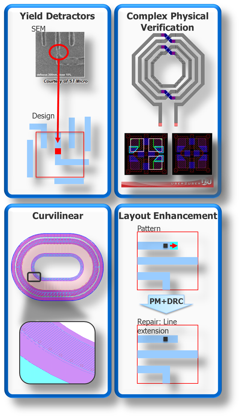
(Image courtesy Mentor Graphics)
Identifying yield detractors is the most obvious application: layout issues learned from systematic yield losses and traced back to a particular arrangement of polygons. But you may also want to be sure that some more complex beast is correctly constructed. The figure up there shows an antennae-y, twisted pair-y thing. If you wanted to define that by all of the dimensions, well… good luck. And it doesn’t have to be a “bizarre” cell like this (bizarre to a logic dude, anyway); you might define a memory cell as a pattern. We’ll come back to that a couple more times.
As to the curvilinear thing, defining the rules in text would be a mess. Conceptually, at least, using a pattern might be easier. Their final example shows a layout edit – let’s say you want to make a change in the layout at every place where a particular arrangement occurs. Well, you can define a pattern and then have it search for the pattern and make the fix.
Yeah, that’s the other cool thing: you can script things so that, when patterns are found, some action is taken. In theory, when you make that change, the result should be correct by construction, but most of the time, checks are run again afterwards, just to be sure.
So… conceptually, that’s how it’s done. But what does it mean to define a pattern? We tend to think of a pattern as an arrangement of polygons on a layer. And, in fact, you can think of pattern matching as the lithography aperture scanning across the layout, looking for patterns. That “window” – roughly a micron wide – can be centered over a “point of interest,” or PoI. Presumably that PoI has been identified as being of interest for some reason. In particular, if it’s a yield detractor, then there’s some feature that’s more prone to bridging or opening, so that’s where you start.
You’d typically be on a single layer at this point – which makes sense, because lithography happens one layer at a time. From the center of the PoI, you may want to define the entire contents of the window as the pattern, or you may want to “fuzz out” more as you get to the edges to abstract away some of the less relevant features at the edge. Part of me assumes that there might be many features that don’t matter, but, based on this window notion, everything within range is subject to exposure at the same time, and, at these dimensions, it can be argued that everything affects everything else within the range of the exposure.
In some cases, however, you’re going to find that a single layer isn’t enough. You might find a via or contact issue that involves features on multiple layers – metal and via, perhaps. What then? No problem; you can do that. Patterns can involve more than one layer. In this case, there may be two or three layers in the mix.
But let’s go back to that thing where a memory cell (or some other circuit) is defined as a pattern for the purposes of physical verification. In that case, you need to include all layers (or many layers). You may have a 40-layer Dagwood sandwich as your pattern.
So, by this process, pattern by pattern, you populate a pattern database. On a new process, you’re going to follow a learning curve: lots of new patterns early on, with the rate of new pattern addition tailing off as you get more experience on that node. Although Mr. White says that there are always a few more trickling in; it never completely stops.
This database will be proprietary to a particular fab or foundry. Yeah, on the one hand, multiple groups of people are off doing the same thing, which might sound inefficient. But the reality is that each process and each foundry will have its own particular issues to look for. There’s probably a lot of overlap between databases, but there will presumably also be a lot of non-overlap. So these databases aren’t public and aren’t shared.
With a database in place, you can now run checks on a layout. Again, it stimulates the question, how does that actually work? What is clear is that the software scans across the layout, much as a stepper would, checking the database for matching patterns. It’s that window thing.
But it got me thinking: you scan to a location and check for patterns. Then you step right and check again. Does that mean that for each step, you have to check the entire pattern database? That sounds like a ton of work. Of course, in this case, you don’t have a real, physical stepper; this is a virtual notion. You have a series of coordinates that need to be checked. In theory, you could assign each scan position to a different processor to run in parallel – as long as the pattern database was replicated or shared in a way that kept access from being become a bottleneck.
But that’s just me speculating. What does Mentor say about this? Yeah, this is where we get into secret sauce territory, so we’ll have to leave it at speculation. Mr. White confirms that whatever they do is well suited to parallel implementation, but that’s about it.
There’s one more layer, so to speak, that goes into this whole process: the notion of waivers. As in, you get a bunch of flagged patterns, some of which you fix, but others you decide are OK and you waive them (recording that fact so you don’t have to do it over and over again every time a check is run).
But there are times when you might have too many waivers and just decide to punt on the pattern matching for some circuit. Our memory cell is an example of this: those cells are carefully crafted, and they may include things that are violations but have been deemed ok in the context of this specific memory cell.
The simplistic way to handle that – and yes, this is done – is to mask out the memory array during pattern matching. Problem is, if there are any true problems in the layout, you won’t find them because, in your desire to mask out all the false positives, you’re also masking out the true positives.
In order to get rid of this problem, cells can be defined with built-in auto-waivers. That memory cell with a bunch of different violations? You waive them all in the cell definition. Then you don’t have to mask out the cell in its entirety; you go ahead and check it. Pre-waived issues won’t be flagged; real issues will.
So that’s the run-down on pattern matching. I wish I could give you an auto-waiver for the next time he or she asks you what color their eyes are, but that’s DRC; you’re on your own there.


Can you envision other applications for pattern matching technology?