


3D NAND embodies the new vertical scaling direction for flash memory. We’ve heard about it for a while, at least in terms of what the concept is. But we’re just now getting “proofs of existence” and lower-level details on how you actually build such a beast.
At last month’s IEDM, I had a conversation with Micron’s Chuck Dennison. He was coauthor of a paper describing the joint Micron/Intel 3D NAND project. This gave a more detailed picture of how they managed their process.
As a general quick review, the whole idea here is that 2D scaling of flash memory is running out of steam. So the memory string is being flipped vertical. But rather than doing multiple standard silicon layers, with litho steps required for each layer (which would be expensive), thin films are stacked up and then holes are drilled all the way through all the layers at once. Those holes are then filled with concentric layers that form a transistor.
Micron/Intel’s 3D architecture
Turns out there are a couple of ways to approach this. One has horizontal channels (in the context of a vertical stack); the other has vertical channels.
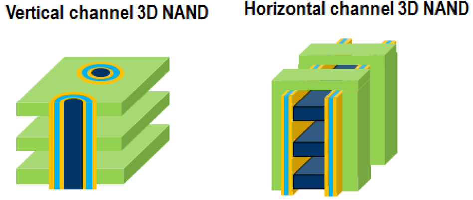
Image courtesy IEDM
According to Mr. Dennison, the horizontal channel version gives a smaller effective cell area, but the vertical version has better electrostatic control and cell on-current because it has a larger effective gate width. Macronix is choosing horizontal; Micron/Intel went vertical.
There’s another technology choice that can be made: floating gate vs. charge trap. With floating gate technology, you tunnel electrons onto an isolated gate from which they can’t escape (easily) unless erase conditions are set up (although a few leak off over time – hence the data retention spec). This is familiar from 2D flash.
By contrast, with charge trapping, the electrons don’t end up in a conductive material like a floating gate; they are embedded into oxide. There has been some work on the latter resulting in some production of small memories, but mostly it’s still a research topic. Micron/Intel went with floating gate.
What’s unique about their architecture is that they build the cell array floating above the control logic. They do this by growing an N+ layer over the word select and other logic functions, so the cell array transistor source, which would normally be in the bulk silicon, is instead its own layer – which allows it to be biased to a level other than where the bulk is. As we’ll see, this helps with erasure.
With that setup, then, you can see below the steps for building their structure.
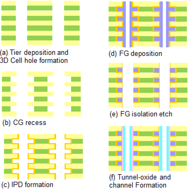
Image courtesy IEDM
The alternating films (polysilicon and silicon dioxide) are first laid down; this work uses 32 layers (each layer is a pair of films), plus dummy layers and a select gate layer. The cell holes are then drilled all the way through (a). A selective etch is then done to recess the conductive layers in order to make room for the floating gate (b). At that point, inter-poly dielectric (IPD) is deposited (c), followed by the floating gate (d). The excess floating-gate polysilicon is then etched away (e), leaving isolated floating gates in the recesses created in step (b). Finally, the tunnel oxide is deposited as the outer cylindrical layer, with the channel filling in at the end (f).
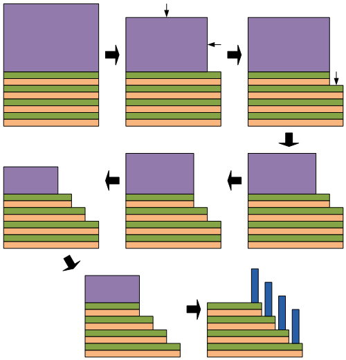
An important part of 3D NAND is how you access the word lines. This is done by a characteristic stair-step structure that exposes each word line and allows a connection to it. The process that creates this could require, in this case, 32 masking steps, which would again be really expensive. Instead, the process can theoretically be done with a single litho step (although some are doing a subset of layers with one mask, then using another mask before continuing to correct for any accumulating errors).
This isn’t novel for Micron/Intel’s particular 3D NAND, so it’s not covered in their paper. But I figured I’d describe it anyway, since it’s also a unique – and critical and difficult – aspect of 3D NAND. It involves a so-called pull-back etch. What this boils down to is a big blob of resist that is selectively etched to expose a controlled portion of what it’s lying on. Those exposed layers are then selectively etched.
Then the resist is “pulled in” again – etched further, which exposes a little more of the underlying films. (Note that the top of the resist is also etched each time, meaning you need a thick layer to make sure you can do all the layers without running out of resist.) Then you etch the exposed films again – which continues the etch already done on the first exposed portion.
The etches need to be done carefully to ensure that they stop at the boundary of the layer being etched – that is, when new material is uncovered. Once all the stairs are complete, connections can be made (I haven’t detailed that portion). A super-simplified rendition of this is shown below.
Programming and Erasing
When programming, the source takes on the normal low voltage that you would expect. But when erasing, because the source is distinct from the bulk, it can be raised to a high voltage, with the select gate going to an almost-as-high voltage and the control gates grounded. Effectively, you’re turning the transistors upside down, where the source acts like a drain.
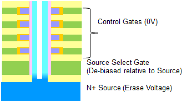
Image courtesy IEDM
They also had to make sure that neighboring cells don’t interfere with each other. That’s partly handled by an “inhibit” voltage placed on neighboring strings. In addition, 2D cells have leakage paths that don’t exist in this 3D structure because of the gate-all-around configuration; there’s nowhere for the leakage to go.
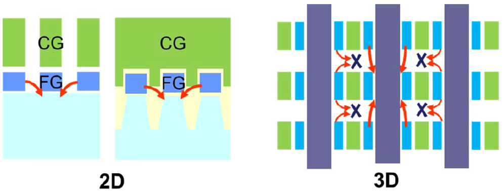
Image courtesy IEDM
The fact that they could place logic under the array had a couple of benefits. First, the word line decoders could be placed under their word lines, making for a shorter connection. Second, they had a lot of area available for that buried logic, so they were able to change the architecture to provide for more parallelism and, hence, higher bandwidth (details not disclosed).
The “program/erase window” – effectively, the voltage difference between a programmed and an erased state – was over 10 V. With that much space, they could start dividing it up do to more than one bit per cell. 2 bits per cell (MLC*) yielded 256 Gb; 3 bits per cell (TLC) got them 384 Gb.
I could tell in the conversation that Micron and Intel are being very careful exactly what they disclose. When I would ask a question, I could see the wheels turning: “How much can I disclose in answering that question?”
Presumably, other details will come out in the fullness of time.
*Apparently, when two-bits/cell was invented, it never occurred to anyone that you’d eventually be able to do more than two bits per cell. So that was called a “multi-level cell,” or MLC. Then when three bits/cell came along, they named that triple-, or three-level cell (TLC). So in this context, “multi” = “two.” “Three” is not “multi.”
More info:
Micron 3D NAND (scroll down)
Intel video (high level)


What do you think of Micron and Intel’s approach to 3D NAND?