


Picture yourself leading a march down the street. If you’re lucky, you’ve got an advance team handling logistics, and traffic has been blocked all around so that there’s nothing to impede your progress.
But imagine now that you come to one particular intersection, and, before you can enter, a few hundred people approach the same intersection from the cross road. They get there before you do, but, rather than passing through and clearing the intersection for you, they start marching back and forth within the intersection.
So when you get to the intersection, you’ve now got this crowd of people in the way, and they’re sticking around. It’s going to be hard – even impossible, if there are too many of them – for your march to make it across. Your procession may eventually give up in frustration.
What the heck does this have to do with anything? Well… let’s back up a few – no, a lot of – steps.
I was at the recent Imec Technology Forum listening to, among other things, a presentation by the formidable An Steegen. If you’ve seen her speak before, you know that you better not spend a lot of time thinking or writing or else you’ll miss something.
The overall topic was the Internet of Things (IoT), and she was tying all the different technology angles they’re working on to how they help to meet IoT imperatives. That includes transistors. Not just smaller FinFETs – like IBM just announced for the 7-nm node – but gate-all-around (GAA) and vertical-gate transistors (which they call VFETs and I like to call PinFETs).
And she put up this graph showing power vs. performance – the idea being that you want low delays with low power – and it had a bunch of different technologies placed here and there. The most promising, in her estimation, was the tunnel FET technology they’re working on. After all, reducing current is a big thing, and if you can do logic with only tunnel currents, that could be a big win.
But something else jumped out at me – something they’re actually not directly involved in. It was a word I’d never heard of before: “spinwave.” And she briefly showed how much more compact a spinwave-based full adder could be, with a hundredfold better energy efficiency than CMOS.
Once back home, I did a little poking around and discovered a whole new world that I had no idea existed. We’ve looked at “spintronics” before in MRAMs, but this is a different deal.
Who knew that a strip of ferromagnetic material could act like a riled-up football crowd. Give the materials the right nudge, and you send a spin wave down the strip. You might consider this to be the magnetic equivalent of photonics – and, in fact, it’s called magnonics. And, just like electromagnetic waves are quantized into photons and crystal vibrations are quantized into quasi-particles called phonons, so spin waves are quantized into quasi-particles called magnons. (I’m sure there’s a cro-magnon joke in there somewhere, but it’s eluding me at the moment…)
And, while the effect involves the spin of electrons and their contribution to magnetic moment, it involves no movement of electrons. In fact, no real particle moves at all. Only information moves – and can do so with less energy stimulus than you need to get an electron up off its butt.
There’s only one catch: these magnons don’t have much of a sense of urgency. Their propagation speed is on the order of 1% of the speed of light (and, apparently, much more subject to attenuation along the way). This is presumably why it didn’t make it into the sweet spot on Imec’s chart. And it’s been the limiting factor. Note that we’re not talking about the speed of a computation; we’re talking about simple propagation delay, meaning that your layout and length of “wire” dominates performance.
If that could be overcome, how would we do useful work with this technology? It’s one thing to stimulate a wave; it’s another to compute. Something as simple as a pass gate can be implemented by running a line over the magnetic material (separated by a dielectric) and using a voltage to disrupt the wave – a mix of electrical and magnonic effects. And there have been early attempts at implementing basic logic functions, but many of them also involved a mix of electrical and magnonic interactions, including having to convert back and forth between the electrical and magnonic domains (never an efficient way to live life).
A more recent project at the Kaiserslautern Technical University took on the task of implementing an all-magnonic circuit. The idea, then, just as with photonics, would be to translate once from electrical to magnonic, do the desired work, and then translate the final output back to electrical. None of this back-and-forth stuff. A look at their work helps give a flavor to this whole magnonics thing.
Key to implementing logic is a basic transistor. But to motivate how this transistor works, we need to revisit a slightly familiar concept: the Bragg (or Bragg-like) grating. Turns out that, here again, you can put ridges in the ferromagnetic material to do some filtering. In this case, the grating causes a particular wavelength of magnonic current to be completely reflected. In other words, there’s a band gap that can be exploited. The frequency in this case corresponds to the frequency of precession of magnetic moments, whose allowed values depend on the material and geometries.
So let’s set up a grooved channel between a source and a drain, through which a basic source magnonic current can flow. If the frequency is not near the band gap, the magnons can proceed straight through with little loss (you get some minor scattering from the grooves). But then, from the side, let’s say you inject different magnons within the band gap frequency range. We’ll call these gate magnons, and the area where they play we’ll call the gate. Because of the grating, those gate magnons cannot pass through and will reflect back and forth within the gate region, totally cluttering it up for the source/drain current.
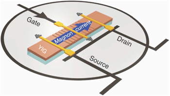
(Image courtesy of the paper author and Nature)
As a result, the source magnon current that was flowing so easily before has to pick its way through all these interloping gate magnons, with so much scattering that you shut down (or partially shut down) the drain current because the poor source magnons simply get fed up and throw in the towel.
Just like our marching scenario above.
So by controlling that gate magnon current, you modulate the source/drain magnon current in the same way that a traditional FET modulates an electron current.
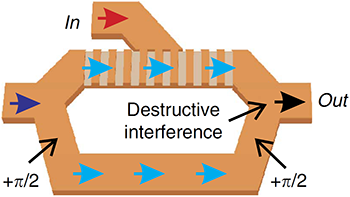
The Kaiserslautern team took things a few steps further to show both analog amplification and an XOR gate. The amplification comes by splitting a current and inverting one side so that, when brought back together again, they interfere destructively. So, while this runs, there’s no output. But if you have a transistor on one side, then you can partially (or totally) shut down the current on that side, making the interference less than total and resulting in a (presumably higher-energy) signal that mimics the transistor gate control.
(Image courtesy of the paper author and Nature)
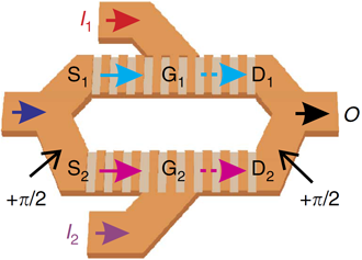
You can use the same effect digitally with a transistor on both sides to allow either one or the other signal out (a logic 1) if either of the transistors is on, or no signal (a logic 0) if neither transistor is on (meaning interference kills the signal) or if both transistors are on (in which case both sides are squelched). In other words, you’ve got an XOR gate.
(Image courtesy of the paper author and Nature)
Bear in mind, however, that the transition times for turning these transistors on and off is on the order of 100 ns or so – not the speediest thing ever. But the goal of this project was to implement a commercially viable all-magnonic circuit. It’s not optimized.
Not sure whether this will ever be a mainstream technology, but the parallels with photonics felt pretty dang compelling to me. This particular paper is also a couple of years old, so I guess it’s one more thing to keep an eye open for. We may revisit this again if developments warrant.
More info:
Magnon transistor for all-magnon data processing


Do you see spin wave circuits in your future?