

Mechanical switches are as old as, well, electricity. Whether you picture the giant two-handed switches in horror movies or the simple wall switches in our houses, we’re used to making contact metal-to-metal.
So transistors used as switches, as old as they may seem, are the newcomers. The thing is, they can be made so small that, within the world of digital logic, we’ve never looked back at their mechanical predecessors – until now.
The advent of MEMS and NEMS technology is bringing mechanical concepts, which have been on the sidelines for years, back into the discussion. But simply scaling down a macro switch into a micro or nano version doesn’t quite work. There are forces at play – literally – in this tiny realm that you just don’t notice in the macro world.
The poster child for this is stiction. You can build, say, a cantilever and use a voltage applied at the end to bend it down until it makes contact with the substrate. The problem is, likely as not, when you remove the voltage, the cantilever will not spring back up to open the switch; it will stick in the closed position due to low-level molecular forces. This is stiction.
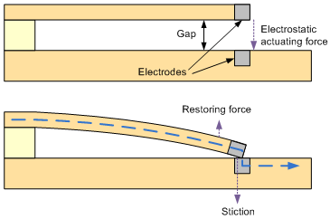
Figure 1. Traditional cantilever switches get stuck in the “on” state due to stiction.
You can reduce the stiction by increasing the switch gap, but then you need a higher voltage to close the gap. There’s no obvious way both to achieve a low actuating voltage and to reduce stiction to a negligible level.
At least, not with an empty gap. A team at MIT led by Farnaz Niroui added an interesting twist to eliminate stiction. In concept, it’s extremely simple: fill the gap with an elastic material. If the gap is narrow enough, a tunneling current will result. In the manner of tunneling currents, if you actuate the switch and squeeze the goop in the gap, the gap may not close by much, but the tunneling current will increase by orders of magnitude.
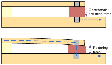
Figure 2. The “squitch” concept: an elastic material in the gap conducts tunneling current.
And when releasing the switch, the goop, being elastic, pushes the electrodes back apart through its restoring force. Look Mom, no stiction!
Because this is a switch that works by squishing this gap material, they refer to it as a “squitch.”
The way they built this is a bit different from how I’ve depicted it in the above conceptual figures. Instead of the traditional horizontal cantilever, they built a vertical one. And there are a few tricks behind how they did this.
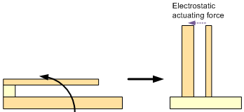
Figure 3. Squitch is built vertically.
The first trick comes with the PMMA photoresist they use to define the cantilever. They lay down 5 layers, with the lowest ones having lower molecular weight. If they were all the same, then you’d simply get vertical walls. But the difference in molecular weight causes an underetch, with the following resulting shape. This will be important in the next step.
The gap between the electrodes at this point is 15 nm.
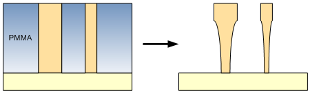
Figure 4. Lower molecular density in the PMMA photoresist at the bottom results in undercuts.
Next, the device is swaddled in gold, as if it had earned the ire of Goldfinger himself. Gold is important because the polymer used in the gap has an affinity for gold. So we want it there, but it ends up everywhere.
Or almost so. If it were truly everywhere, then we’d have a problem. These two electrodes on each arm of the cantilever need to be electrically isolated, or else we can’t use an electrostatic force to close it. In fact, with gold everywhere, everything would be connected to everything, so we would effectively have created gold bullion with a soft silicon center. Nice as a paperweight; not so great as a circuit.
This is where that undercut comes in: it shadows the gold deposition, keeping the gold away from the undercut surfaces. This ensures the isolation we need between the electrodes (and between the electrodes and the rest of the chip).
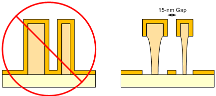
Figure 5. The undercuts ensure that the deposited gold doesn’t short out the electrodes.
Finally comes the deposition of the magic material that will fill the gap. And… there are some odd things that happen here, and I’m not exactly sure of the order in which they happen nor the exact mechanical mechanism at play. (I’m not sure if the research team even knows the specifics.)
The material itself is thiol-based, meaning it uses sulfur: fluorinated decanethiol. The molecule has end groups that have an affinity for gold, and they self-assemble into the gap. Somewhere along the way, one of the electrodes “collapses” towards the other, with a resulting gap of about 1 nm – much narrower than could be patterned lithographically. And the gap is now filled, with a gold/goop/gold “stack.”
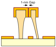
Figure 6. A finished squitch, after deposition of the fluorinated decanethiol film and electrode collapse.
They built and tested two versions of this. One had no material in the gap – and no gap collapse – because they didn’t take it through the last step, meaning that the gap was still 15 nm. Testing it as a switch, they were able to close that gap by applying about 4 V, but it worked only once: after that first contact, the stiction was stronger than the restoring force of the cantilever, and so it remained irreversibly closed.
The other version they built was taken through that final step, and so it had the material in the gap. It was able to open and close reliably, requiring only around 1.5 V for complete closure (consistent with a narrower gap, although it’s also working to squish the fluorinated decanethiol).
All of this leads to the question, how would you use this? My idle ruminations identify three possible scenarios that might be considered: use for switching low-current circuits; use for switching high-current circuits; and use for switching RF circuits (or anything where frequency content matters).
Tunneling currents are low, almost by definition. If the circuits being switched need only low currents, then they could conceivably be switched directly with squitches. This could work where, for instance, the switches are used to store configuration information.
If, on the other hand, higher currents were being switched, the squitch itself might not be able to conduct that current, so… you’d have to sense the difference and then activate some other switch that conducted the actual current. Which raises the question… what would you use for that other switch? And how much sensing circuitry would be needed? The conclusion I come to is that this wouldn’t turn out to be effective. (But I could be wrong….)
Finally, if the purpose of the switch is to transfer signals where information resides in the frequency content, like RF signals, then I would think that more study is needed. It all depends on how the fluorinated decanethiol affects that signal. If it acts as a filter (which, in all likelihood, it would), is it going to eliminate information at critical frequencies?
One last thought about power consumption: presumably, the gap in a traditional cantilever is wide enough that the off current can be considered exactly zero. A squitch, by contrast, conducts whether on or off. The off current is on the order of nanoamps or tens of nanoamps, which is small, but it represents a non-zero leakage current that might make a difference to someone trying to conserve every last drop of energy.
These practical considerations will presumably have a voice in determining the future of the squitch (including possible future research modifications). But it’s hard to deny the elegance of the idea.
More info:
Nanoelectromechanical Tunneling Switches Based on Self-Assembled Molecular Layers (behind a paywall)
[Editor’s note: link has been edited; original link was incorrect]


What do you think about MIT’s stictionless switch?