


There’s the textbook version of the tech business, where hard-working innovators push the edges of technology, bringing ever-more-efficient products into a free market where consumers reward those who best meet consumer needs.
And then there’s the real world, where “innovation” can sometimes mean finding the cleverest ways to cheat.
I mean, yeah, I know that bad guys are out there trying to steal our identities and more. And that shortcuts will always be taken by some. But I have to admit that, as I sat through an ICCAD session on hardware security, the scale of things surprised me.
The litany of ways in which companies try to pilfer or sabotage other companies’ innovation is striking. These kinds of “attacks” involve non-trivial equipment and access to confidential materials. The folks conjuring up defenses lay out scenarios involving miscreants that may have:
- Access to the die (not too hard to imagine), including internal nodes
- Expensive probing equipment that can force and measure internal nodes
- Access to serious computing resources for guessing or reverse-engineering keys
- Access to critical design documents: schematics, gate-level netlists, RTL
- Access to critical test documents: test vectors and their expected outcomes
- Moles placed in the design team of a competitor – they can provide information or install back doors in the chips.
And after all that, your manufacturer might make a few extra pieces on the side and then sell them on the sly for a few extra bucks.
While the scope of activity is wide, it left me wondering how common this activity is (I do often drink the “innovation always wins” Kool-Aid). It certainly happens enough to warrant studies of ways to thwart such attacks. We hear often about software vulnerabilities, but hardware is even more fundamental. Security in the Internet of Things in particular has been neglected for too long, and notes of caution and outright concern are being sounded. Without secure hardware, little else matters.
Three different ideas were put forward in three different presentations at ICCAD. The first two involve locking and obfuscating a design; the third involved dealing with “Trojan side channels” (TSCs). A walk through the activities provides some insights into this spy-vs-spy world.
Lock it down
The idea of locking a design is pretty simple: if you don’t “activate” a circuit with the right key, then the circuit simply won’t work right. In theory, that means that unauthorized copies of chips shouldn’t work because they haven’t been properly unlocked. Which raises a question about where the unlocking happens, but we’ll get to that in a minute.
A team from the Howard Hughes Medical Institute (HHMI) and the University of Michigan took a look at what’s called the EPIC approach to locking a circuit, established some vulnerabilities, and proposed some improvements.
EPIC involves sprinkling XOR or XNOR gates throughout a circuit. One input to the XOR would come from a circuit node, the other from a key. The XOR output drives the load that the circuit node was driving in the original circuit. It’s a straightforward bump in the wire.
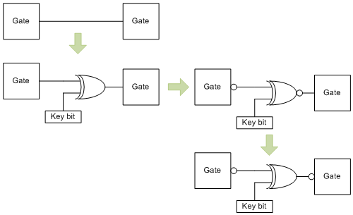
The idea is to leverage the XOR gate’s role as a programmable inverter. If the key has the wrong value, then the original signal will be delivered inverted, which will screw up operation. You can then play other inverter games, using XNOR and then pushing the inversions around in an attempt to make it less clear where these key bits are to anyone studying the schematic or actual die.
For this to work, the key must be inaccessible to nefarious folk. Depending on how much access they have, however, they may be able to probe the die to reverse engineer or guess the key, or they might be able to intercept the key when it’s delivered for activation – when the key is loaded. That last one becomes a manufacturing concern: who has access to the key to unlock the chip?
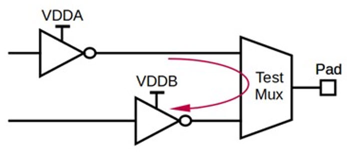
With a locking strategy like this, it’s safest not to activate the circuit in the fab where the key could be sniffed; you want to have activation as a separate step by a separate entity – a divide-and-conquer strategy. But there’s a problem: you have to test the circuit, and this is typically done in the fab (at least in wafer form). And in order for the tests to pass, the circuit has to work.
In other words, you need to activate the circuit before testing. Which means fab activation. Which is a vulnerability. Meanwhile, the team showed that EPIC could be attacked through an algorithm that walks through key guesses, gradually locking down individual bits (since they’re independent of each other) until they cracked it.
In other words, this approach is vulnerable both through reverse engineering and through activation.
The team’s improvement came through a refinement of how and where XORs are placed. The fundamental idea is that test should work without the key – that is, no activation would be required before test.
That means that the XORs have to be inserted in such a way that they happen to cause correct values when stimulated with test vector inputs while causing incorrect values for other conditions that don’t happen to be in the test vectors.
There’s one obvious concern here: you need the test vectors while doing the design – probably earlier than the test vectors might ordinarily be available. And these XORs are hard-baked into the circuit, so vector changes could be problematic.
Obviously, removing vectors won’t cause a problem. If you add vectors, however, and you happen to activate a state where the XOR inverts the internal signal, then you’ve got a problem. This method creates a much tighter interdependency between the test and design than might be typical, and it raises the risk of a mask change if test vectors evolve after the design is locked down.
PUF obfuscation
UCLA took a different approach. Their approach was not to disable the circuit in the absence of a key, but rather to obfuscate as much logic as possible to thwart reverse engineering attempts. Rather than relying on a vulnerable external key, they relied on physically-unclonable functions (PUFs). We covered PUFs several years ago, but there are some new nuances in the more recent works.
As a quick review, the idea of a PUF is that every circuit has slight idiosyncrasies, based on process and other variations, that make the chip unique. The trick is in finding and harnessing the best such phenomena.
The ones we talked about before – some of the earliest to be implemented – tended to rely on SRAM power-up states. Each bit can power up high or low, and slight variations will bias each bit slightly differently from the same bit in another chip that has the same design. If you get enough bits, then you get a power-up signature (with ECC to correct noise) that’s unique to the chip. That signature can be used as a key.
Because each chip will therefore have a different key, there is far less value in trying to guess keys. Even if you guess one, it will work only for the one chip. That could still be a problem, but it does prevent someone emailing a key around to unlock all instances of the chip.
But there is an inconvenience involved in this scheme: it requires power-up to generate the key. Since then, some PUF circuits have been proposed that can be activated while the circuit is powered up. This allows key generation or validation without power cycling.
The PUF implementation that came up in several presentations originated at MIT and looks more or less as follows:
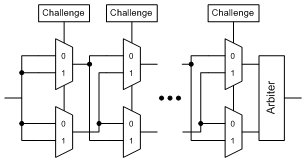
The arbiter is, in simplest forms, a D flip-flop, with one input driving the data and the other driving the clock. If a rising-edge signal is applied at the input, then, depending on which muxes direct which signals in which direction (as determined by the challenge bits), and, depending on the specific delays for the individual chip, then either the data will arrive first, meaning that a 1 is clocked through, or the clock arrives first, meaning the 1 isn’t clocked in. Given sufficient challenge bits, each PUF will have a unique truth table.
Of course, there’s one glaring issue that comes from this. The whole idea is this difference between clock and data signal delays, and the range is a continuum – meaning that it’s entirely possible – even likely – that some of the challenges could cause metastability. And the problematic challenges would vary from chip to chip.
I confirmed with one of the authors that metastability is indeed an issue. But there are methods for accommodating it. One can design the challenge set in a way that avoids metastable states. Or, for example, the arbiter might contain a 3-way voting circuit in which the same challenge is presented three times, and two out of three wins.
So each PUF can be characterized across the challenge space The map of which challenges result in 0s, which result in 1s, and which are unstable constitutes a unique signature truth table if the space is large enough.
The obfuscation idea is to take some logic and, instead of implementing it outright, implement it in an FPGA. But the FPGA doesn’t generate the output directly; it generates an input to the PUF; the PUF will complete the calculation. Because the PUF is going to create behavior unique to the chip, the FPGA design not only has to incorporate the desired logic, but it must also “reverse out” or “pre-equalize” the effects of the PUF. You might think of the PUF as having a chip-unique transfer function and the FPGA as containing the desired logic multiplied by the inverse of the PUF transfer function.
In other words, the FPGA pattern will need to be unique for each chip.
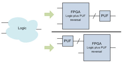
By putting the FPGA first, the synthesis algorithm can be sure to avoid having the FPGA generate any combinations of signals into the PUF that might cause metastability. If no such instability exists in the PUF, then it’s actually preferable to reverse the order – have the PUF come first. This is said to make the PUF outputs inaccessible to someone trying to crack the PUF, improving security.
Note also that, in this case, you can use some subset of the inputs into the PUF, combining the remaining inputs in the FPGA. In that case, the PUF reversal impacts only a subset of the logic; the logic involving the extra inputs would be in the clear (although hard to detect).
So the huge question here is, how do you incorporate this into a manufacturing flow? In order for this to work, you have to:
- Characterize the PUFs on each individual chip.
- Synthesize the logic for the various FPGA blocks for each chip, individually, according to the characteristics of the PUF.
- Program the FPGA blocks for each individual chip.
- Destroy the PUF characterization circuit access so that no on in the future can re-characterize the PUF.
They also talk about accounting for PUF states that might not be metastable, but might be very sensitive to environmental variation – voltage and temperature in particular. Such states would be a problem since operational conditions would likely not match test conditions. If that had to be characterized as well, that makes the problem even harder.
This certainly involves steps and tools that aren’t a traditional part of a test environment, and they will add to test time (which means adding to cost). While technically interesting, this would probably need some refinement before being ready for a high-volume manufacturing environment.
A different kind of obfuscation allows a PUF to reverse wires.
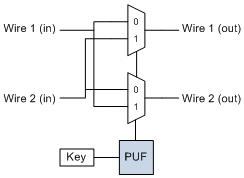
If a key is n bits wide, then there are 2n possible combinations, one of which will presumably be used as a key (stored non-volatilely after PUF characterization, presumably). The key obviously has to be one of the PUF inputs that routes the signals correctly. But there may be many such values – it seems like, across all PUFs, ignoring metastability, there should be a 50/50 chance of any random input working. But sprinkled liberally throughout a die (avoiding critical paths), the idea is to overwhelm anyone trying to reverse engineer the thing by the sheer number of possible combinations.
When using these techniques, they recommend locating the PUFs in places that would be hard for an attacker to access – nodes that drive and are driven by many flip-flops (high fan-in and fan-out), for instance, where their values can’t be easily forced. It’s also preferable to use inputs that are highly correlated. In the wire-swapping case, it’s also good to build long chains of swaps feeding swaps. The general idea is to make it as hard as possible to generate truth tables if someone manages to get in there with a probe. Yeah, that would be some serious reverse engineering.
Looking Gift Trojans in the Mouth
Finally, another paper from the Chinese University of Hong Kong and Tsinghua University of Taiwan dealt with so-called Trojan side channels (TSCs). Side channels can refer, for instance, to variations in power that can be analyzed and decoded to compromise the cryptographic engines. It’s been long known that such side channels might unintentionally divulge clues about internal chip activity, but the scenario here is worse: it involves someone literally building such a channel into the chip, unbeknownst to the project managers.
They focus on one specific type of side channel, called MOLES, which uses “leakage modules” to modulate the power. The key bits (or a subset of the key bits) in the crypto engine might each be connected to a leakage module, changing current according to the bit value. The problem this team addressed was not how to defeat such an attack, but merely to identify whether a circuit had such side channels and, if so, which key bits were involved.
I’ll let the paper speak for itself as to the details of the detection algorithm. But the thing that really got me here was the fact that design teams could include folks that are intentionally adding circuitry to defeat the security of the chip. And that you might need a special super-secret test on your first silicon to see if it’s been compromised. Straight out of James Bond.
It brings to mind requirements-tracking processes used for safety-critical design, such as DO-254. One general tenet of such methodologies is that every design requirement has associated circuitry, and every circuit has an associated requirement. In theory, a thorough implementation of such a process would expose extra circuits.
But such discipline tends to involve extra work and time. While those processes are tolerated for safety-critical designs, it’s hard to imagine them being used for high-volume, highly competitive consumer products.
The main non-technical takeaway here is that there’s a dirty underside to the design and manufacturing of electronics. Probably not a huge surprise, but the time and effort and chip area needed to thwart these techniques are a distraction from doing useful work.
But IP and secrets are valuable, and sometimes you’ve simply got to spend some time fixing the locks on the doors to make sure no one can get in and steal the goods. Ultimately, if you can’t trust the hardware, then you can’t trust the software. And if consumers can’t trust, then they probably won’t buy.
More info:
Protecting Integrated Circuits from Piracy with Test-aware Logic Locking
Hardware Obfuscation using PUF-based Logic
On Trojan Side Channel Design and Identification


What do you think about these hardware security ideas? Worth the cost? Manufacturable in volume?