


The Americans with Disabilities Act (ADA) had resulted in marked improvements in his ability to access the people and places and resources that normatively-abled people took for granted. Curb cuts, wider paths, and ramps instead of stairs all meant that his wheelchair could go much farther than was previously possible.
But it wasn’t perfect. A cozy coffee shop might, for instance, have only a few tables near the entrance that a wheelchair could reach. They weren’t “handicapped only” tables; they were just near the door, and the tables farther in were too close together to allow passage.
So it was common for him to arrive, only to find that the tables that he could use were occupied (even while tables in the back were empty). In which case he had either to wait or to move on.
Now… if only he could call ahead to the coffee shop to let them know he was coming. They could then reserve one of those tables to ensure that, when he arrived, one was available. Then everyone – including him – would be able to get a table.
As engineers, we’re taught the stability of the feedback loop. (If we mind our poles and zeros, that is…) Just sending something on, without feedback to provide corrections, is a recipe for escalating error.
Perhaps this is why, instinctively, our approaches to process control always focus on feedback loops.
Specifically, in a fab, one of the reasons for monitoring wafers is to get performance information on the steps already completed. If something doesn’t look right, it’s an indication that one of those steps wasn’t done optimally. The assumption is that, if it wasn’t right a few minutes ago, then it’s probably still not right, and we should use this info to apply some kind of correction and make it right. That’s exactly how feedback is supposed to work.
Well, that correction is great for the subsequent wafers; they’ll be processed more cleanly than the one(s) that triggered the correction. But what about those off-center wafers? What to do with them? They might be marginal now; can they be processed further and salvaged (perhaps with crappy, but non-zero, yield)? Or might the next steps compound the problem?
If things are just going to get worse, then you might as well toss the things now rather than spending more money on inevitable failures.
But here’s the thing: if the following process steps knew something about the state of these wafers, they might be able to compensate and rehabilitate them. And that works not only for wafers that are questionable: with the amount of variation possible during processing, and with decreasing tolerance of variations, this can be a way of widening the process window so that more variation can be accommodated.
We do this by feeding the data from the wafers forward to the next piece of equipment so that it knows something about the wafer it’s about to process. It’s calling ahead to the next step to let it know what’s coming.
This is the essence of what KLA-Tencor is calling its “5D” program, recently announced. That nomer is something of a loose marketing concept that incorporates the following:
- Overall increased process difficulty, as embodied most dramatically in 3D structures: FinFETs and 3D NAND. This gets 3 of the 5D.
- The fourth dimension is time. I guess that’s not news. But, specifically, it means processing time. As in, less is better.
- The fifth dimension is a 1960s musical group. But, in other news, KLA-Tencor has applied this notion to cost. Again, less is better.
Specifically, they’re announcing 3 tools (OK, 2 new tools and one update) to enable this feed-forward concept. Let’s dig in a bit deeper on how the time and cost dimensions work.
One of the main contributors to increasing process complexity is multiple patterning. We’ve talked about it before, but, in summary, it lets us take a single pattern, break it into two half-patterns, and then expose them one after the other. The result should – ideally – be the same as if we had exposed it all at one time with a full pattern on a single mask. Which we would do if the structures weren’t too danged close together.
The only way this will work is if we align the second half-mask as closely as possible over the first half-mask’s already-exposed pattern. We refer to this as “overlay.” And it’s going to get harder, what with quadruple patterning on its way.
The problem is that overlay convolutes an already increasingly tight process. We measure our process success by checking various “critical dimensions” (CDs) to make sure things are in spec. And, unless you’re in the middle of this, it may come as a surprise some of the things that can mess CDs up.
Things like “wafer shape.” We blithely think of wafers as nice, perfectly flat canvases for our silicon creations. But, in fact, they’re not exactly flat. Yeah, we try to make them as flat as possible, but there may be slight warpage due, for instance, to various stresses from applied films or higher-temperature processes that might not yet have relaxed out completely. Or there might be very slight thickness changes across the wafer.
Granted, we’re talking minute deviations, but they can have an impact. If a “scanner,” which exposes the patterns on to the wafer, is set to a fixed focal distance, then these slight ripples or dimples in the wafer can move the surface above or below the intended focal distance. Which means the exposure is going to be fuzzy on some of the dice, which can result in CD failure.
That’s without considering multi-patterning. Overlay errors can themselves cause yet more CD failure.

Image courtesy KLA-Tencor
KLA-Tencor has proposed to address this using a couple of different tools. First, it’s announcing the WaferSight PWG (patterned wafer geometry) tool. It’s based on an earlier similar tool intended for unpatterned wafers. It measures variations in flatness and thickness of wafers. It can create a map that’s forwarded to the scanner: the scanner can then adjust focus based on this information, keeping much more of the wafer in focus.
The second tool is their LMS IPRO6. It helps with overlay. The traditional way to ensure that one mask is aligned squarely above the patterns already laid down is to include “alignment marks” or “keys” on the wafer. These would typically reside in the “streets” between individual dice on the wafer. The reticle is aligned over these marks.
What KLA-Tencor has found is that they can use actual circuit patterns to improve alignment. This has been done before, using so-called high-order wafer correction, but it’s too slow to use in production because it uses on the order of 1000 sample points. KLA-Tencor found that they can reduce that to around 200 points and extrapolate successfully, making it suitable for production use and, therefore, allowing better overall overlay control.
This information can also be fed to the scanner so that imperfections in individual reticles can be accommodated.
The third product is an update to their K-T Analyzer software (version 9.0); this crunches much of the data required to do this feed-forward thing. The data from the first two tools isn’t sent directly to the scanner; it goes to K-T Analyzer, which munges it all and sends its conclusions to the scanner.
There is still traditional feedback going on here too. KLA-Tencor illustrates how the various tools and data paths interact in the following graphic.
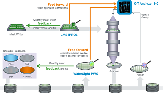
Image courtesy KLA-Tencor
So let’s go back to the 5Ds and see how these improvements help the 4th and 5th Ds. The 4th is time, and, theoretically, we’re adding new monitoring steps to the flow, so this ought to lengthen cycle time. Note that these never become rate-limiting steps, so our process pipeline’s “frequency” isn’t changing – just the latency.
But that counts only if all wafers process perfectly. Then, yes, your overall cycle time increases. But, here in the real world, some wafers end up misprocessed, or they need rework, or they fail due to missed CDs or whatnot. A lot that has to be reworked, for instance, has a much longer cycle time than one that doesn’t. Averaging all the lots gives a cycle time that’s longer than the theoretical one.
The idea is that, by reducing the fallout or the number of wafers that need reprocessing, then, even though you increase (by a little bit) the ideal cycle time, you reduce the typical average cycle time. And so this improves the 4th D.
And cost, the 5th D? The idea there is that you can use this approach to extend the life of existing equipment. Costs are saved both by further amortization of existing tools and by deferred (or reduced) purchases of new tools.
It’s amazing what you can accomplish simply by calling ahead…
More info:


What do you think about KLA-Tencor’s feed-forward approach?