


A silicon wafer will always be patterned with a perfect grid of rectangular dice. It’s so obvious that you don’t even have to think about it. From the very first wafer you saw in school to whatever you’re working with today, they’ve all looked like a well-planned city with edge-to-edge streets.
But did you ever wonder what would happen if you didn’t lay a wafer out that way? Plasma-Therm presented some alternative ideas at the recent MEPTEC MEMS Technology Symposium, suggesting that breaking the rules can have some benefits – although, as always, there are tradeoffs. I should caution that these are largely conceptual ideas that need further vetting, although ON Semiconductor has done some implementation, confirming net benefits for the dice they worked with.
Let’s start by reviewing how we got here. There’s a reason things are the way they are, and it’s remarkably prosaic: it’s because of the saw you use to dice up the wafer (or “singulate,” in the manner of “why use one syllable when three will do?”). The “streets” have to be wide enough to accommodate the width of the saw blade (the “kerf”) with margin for chipping and damage and such. Given all that space, the streets have been a convenient place for test and alignment structures that aren’t needed beyond the wafer level.
And so, to cut the wafer up, you’ve got to be able to run the saw blade back and forth along the streets in both the x and y directions from one end of town to the other. Hence the perfect grid.
There are a couple follow-on “givens” for this situation:
- Dice have to be rectangular.
- The corners of the dice will be sharp, created where the x and y passes of the saw blade intersect.
This has worked well enough for a lot of years, even though there are some downsides to it, such as the potential for chipping damage. We’ve historically accepted these as a natural part of the yield equation; you’re going to lose some dice, and you simply need to minimize the fallout. But, above and beyond such yield considerations, there may also be some opportunity costs to doing things the old way.
Let’s start with the most obvious one: sawing a wafer up is a serial process. You move across the wafer, running the saw back and forth in one direction, and then you rotate 90 degrees and do it again. It’s a double-raster. Even if you’re using a laser instead of a saw, you’re still scanning to get the job done.
What Plasma-Therm is proposing is to replace this serial approach with a parallel process: plasma dicing, where you etch the entire wafer – all the streets – in one step. There are a number of potential benefits to this, although we’ll need to consider the costs as well.
The first opportunity for improvement is throughput, governed by the time required to cut up the wafer. With a saw, that time will depend on the die size: a smaller die means more rows and columns, which means more streets and, therefore, more cuts. So the smaller the die, the longer it takes to dice.
Saw speed is also affected by wafer thickness: for thinner wafers, you need to slow the saw down to keep from damaging the delicate goods. An alternative is to use a laser instead of a saw. It’s still a serial process, but, unlike a saw, you can go faster on thin wafers with a laser because there’s less material to blast through. This relationship is shown in the following graph.
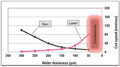
Image courtesy Plasma-Therm
Here you see that the cut speed – how fast the saw or laser can move through the wafer – as a function of wafer thickness. There is a crossover point somewhere around 125 µm thick; thinner wafers favor laser dicing; thicker favor sawing.
Plasma etching also favors thinner wafers, but comparing plasma to saws and lasers is tricky, since there is no cut speed; you’re blasting the entire wafer at once. So Plasma-Therm has calculated an equivalent rate based on 1-mm2 dice on 8” wafers (with some adjustments to account for effects caused by different street widths), and what follows is the same graph as above, but with the plasma dicing added – which totally changes the scale. The equivalent cut rates possible are far faster than what actual saws and lasers do – from the 100 mm/s range to almost 3000 mm/s. This would appear to be a big win from a pure throughput standpoint.
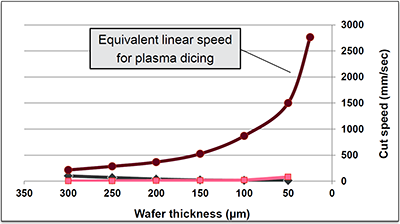
Image courtesy Plasma-Therm
The next advantage comes from the ability to narrow down the streets. In the examples Plasma-Therm showed, they compared 75-µm streets to 15-µm streets – that’s an 80% reduction in street width. What that gives you is one of two things, both of which come as a result of the fact that you’re wasting less space on streets. Most likely, you’ll be able to put more dice on your wafer. Alternatively, you can simply narrow down the streets in place, meaning that, for the same number of dice per wafer, you get a bigger die.
The increase in available dice can be non-trivial, particularly for small dice. For a 20-mm2 die, Plasma-Therm calculates that you get a nominal bump: 2.5% more dice. For a 0.5-mm2 die, however, you can pack 16% more onto the wafer, and smaller yet can get you 30% and more.
To do this, you’ll likely need to move some process control and alignment structures out of the street – meaning you’d replace some actual dice with these structures. ON Semiconductor found that you have to pay attention as you do this: If the structures are too much larger than the actual dice, then they can cause issues if, for example, you need to stretch the tape after the dicing is complete.
Higher throughput and narrower streets are the obvious benefits. More subtle is the fact that you have more flexibility with the shape of your die. No longer do you need a rectangle. You could even pack the wafer tighter with hexagonal dice, honeycomb style. Again, you get more bang for the buck with smaller dice due to the percentage of area devoted to the streets.
Even if you go with rectangles, you can reduce stresses by rounding the corners. No longer do they have to be sharp; they can be any radius you want. This doesn’t affect the number of gross dice on a wafer, but it can improve yield by reducing cracks and breakage around the corners during handling and assembly.
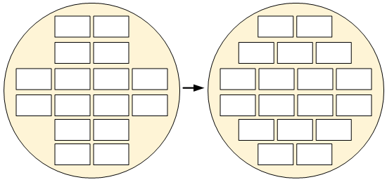
Most of these benefits accrue primarily to small dice. But large dice can also be packed tighter if you give up on the perfect grid – which is no longer needed. In the example below, I can pack in two extra dice by offsetting two of the rows. Two dice might not sound like much, but it’s a 12.5% increase – nothing to sneeze at.
For something more substantial, Plasma-Therm illustrates a CMOS image sensor example where they took a 55×35 mm2 die and increased the die count on a 12” wafer from 14 to 25 – a 75% increase.
One gotcha that occurred to me with this approach comes with multi-die reticles. Given a typical four-die reticle, you can easily expose the wafer on the left above; you can’t do the wafer on the right. Even if you did a two-die reticle (side-by-side), the three-die rows would be messy because you really want 1-1/2 steps, so you’d have an extra dummy die hanging off one or the other side of the wafer.
If that were a problem, you’d have to go with a single-die reticle. The gain in die count would come at the cost of much slower patterning throughput: Moving from a four-die reticle to a one-die reticle would mean a quadrupling of exposure time. This becomes even more of an issue with multi-patterning.
I talked to Plasma-Therm about this, and they pointed out that the dice that benefit most from this will already be too big for a multi-die reticle. In which case you already have a one-die reticle, and there is no impact on lithography throughput.
One other question I posed is whether the litho steppers can be programmed to handle the more complicated pattern on the right. The issue comes when you move from one row to another. Ordinarily, the stepper would perform an x step along a row and then, at the end, perform a y step to start the next row (moving backwards, as the ox plows).
But with the proposed offset rows, changing rows would require both a y step and an x offset (not an x step). And this offset would vary by row, so the machine would need a map of the wafer so that it would know which offsets to perform when. Whether this is possible on existing machines remains an open question.
The final burning question is return on investment (ROI). For example, you may get 10x the throughput, but if it costs you 20x to do that, you’ve gained time but lost money.
This is a key consideration, since the etch process we’re talking about here is deep reactive ion etching (DRIE). It’s an important process both for MEMS and for through-silicon vias (TSVs), but it’s also considered an expensive process. I haven’t seen any specific ROI calculations, but the numbers will depend on the die size, wafer thickness, and yield savings related to mechanical (or laser) sawing. The improved throughput and yield will need to be weighed against the cost of DRIE.
And, of course, any real-world cost numbers depend on your foundry and OSAT (off-shore assembly and test) costs. In other words, there’s no one easy answer for everyone. And I’ve just skimmed the most obvious issues here; Plasma-Therm and ON Semiconductor dig into more detail in a recent webcast. So a clean ROI model appears to be a work in progress.
This concept has the delightful feel of removing long-forgotten shackles and imagining the new possibilities. Whether it pencils out – or, perhaps better said, which situations it pencils out for – is still under evaluation.
More info:
Recent plasma-dicing webcast (registration required)


How do you see the pros and cons of plasma dicing?