

True to my word, I’m highlighting a handful of x86 processors this week. Well, maybe “handful” isn’t appropriate; more like a bushel full. These things are large.
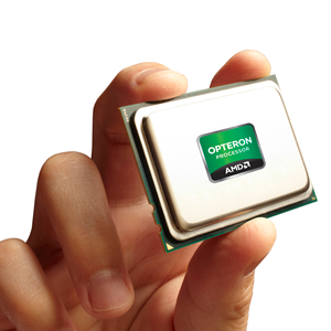
AMD just rolled out a trio of new Opteron chips for embedded systems. It’s not often that you hear “Opteron” and “embedded” in the same sentence, so some clarification is in order here. (Frankly, it’s not often that you hear Opteron mentioned at all, but that’s a different problem.) These are embedded processors in the sense that a Gulfstream V is a small jet. Sure, compared to a 777 it’s a little thing, but the GV is hardly pocket-sized. Smartphone makers need read no further.
If you’re still with us, you’re probably designing or programming systems for telecommunications, networking, medical devices, building infrastructure, or other similarly important, bulky, and valuable equipment. You want a manly processor for your manly gear. No girlie processors need apply here. Everybody grunt with me.
Ready? Let’s git ’er done. The new AMD Opteron parts are server-class processors with some add-ons and take-offs for embedded designers. They’re big and fast 64-bit multicore processors with all the bells and whistles you’d expect from a server or PC chip: built-in floating point, multithreading, three-level caches, MMX, SSE, SSE4, virtualization, overclocking… the works. AMD doesn’t pack on a lot of on-chip peripherals, however, preferring instead to offer high-speed links via two DDR3 memory channels and two HyperTransport 3 links. You can attach AMD’s official support chip and get SATA, PCIe, and all the other goodies that way.
If you’re filling out your AMD roster, the new chips are called Opteron 4386, 4376 HE, and 4310 EE. They slot in between a number of existing Opteron 43xx and 33xx devices, so don’t expect any huge differences. They’re 4- and 8-core processors running at anywhere from 2.2 GHz up to 3.8 GHz. All three have AMD’s “TurboCore” technology, meaning they can overclock themselves for short periods. The boost is considerable, too. The 4376 HE part, for example, is nominally spec’d for 2.6 GHz, but it can sprint at 3.6 GHz for a few seconds at a time. That’s a 1.0 GHz boost—not inconsiderable. Unlike old-school overclocking, however, this is both supported by the chip and controlled by it. That is, the parts will refuse to boost if they sense they’re getting hot. The whole TurboCore feature is based on heat dissipation, not circuit timing paths, so it’s all a matter of balancing performance against thermals. The silicon itself would happily run at the faster speed all day long, if only we could stop converting resistance to heat. Stupid physics.
So what’s the power dissipation really like? To be honest, I don’t even bother measuring the power on high-end processors anymore. It’s not because I can’t handle bench instruments, but just because the results are so application-dependant. AMD says the TDP (thermal design power envelope) for these guys ranges from 35W to 95W. Clearly, they’re for fan-cooled systems, not sealed boxes, but if you’re making an AC-powered product those aren’t terrible numbers. But they’re just ballpark estimates; YMMV. A lot depends on how much external I/O you’re doing. Wiggling those HyperTransport or DDR3 lines expends a lot of joules. And these chips, like all modern processors, cool down quickly if they’re not doing a lot of floating-point math or vector arithmetic. Cache hit rates, program branches, and even the number of decimal places in your floating-point code can all affect their power consumption. That’s why even the EEMBC benchmarks don’t attempt to measure power numbers. (More on EEMBC next month.)
Prices are in the $350–500 range, so we’re talking big iron here. Big branding irons, since the chips require large metal heat sinks and put out a lot of heat, as we’ve mentioned. But all that is fine if you’re building big boxes and want the utmost in performance. The new AMD parts are even socket-compatible with others in the same chip family, so this represents an up- and downgrade path if you were smart enough to design your board to accommodate varying power requirements.
Yeah, they’re big processors, but they’re designed for big jobs. Running Web servers, for example, or RAID farms, or telecom racks that have to pass NEBS testing. They’re not appropriate for handheld devices or pocket gadgets, but something has to power that wireless infrastructure, and I’m glad these chips are up to the job.


