In the last decade we have seen the process of timing signoff become increasingly complex. Initial timing analyses at larger process nodes such as 180nm and 130nm were concerned mostly with operation at worst-case and best-case conditions. The distance between adjacent routing tracks was such that coupling capacitances were marginalized by ground and pin capacitance. Hence, engineers seldom looked at the potential issues associated with cross-coupling and noise effects. It was simply easier to add a small amount of margin than to analyze crosstalk.
Starting at 90nm, and even more prominently at 65nm, an increase in coupling capacitance due to narrower routing pitches and taller metal segment profiles resulted in crosstalk effects becoming a significant concern. In addition, temperature inversion effects began to add to the additional number of analyses that were required to sign off a chip. What started as an analysis of two operational corners increased to at least three corners due to the increased delay at higher temperatures.
At 45nm, process variation for metal layers added to the number of process corners that had to be considered when timing a design. Now at 28nm, the various PVT variations at the gate and interconnect levels, as well as the number of functional and test modes, has increased the number of mode corner combinations into the hundreds. For today’s designs, multi-mode/multi-corner (MMMC) timing analysis is a must.
In this paper we’ll delve more into the details behind the explosion of timing views along with the need to analyze them and, more importantly, optimize timing under all the possible combinations. (A timing view is a combination of one mode and one corner for one timing check, such as setup or hold.) We’ll also take a look at today’s methodologies for addressing these issues and consider how things can be improved.
The Necessity of Increasing Timing Analysis Coverage
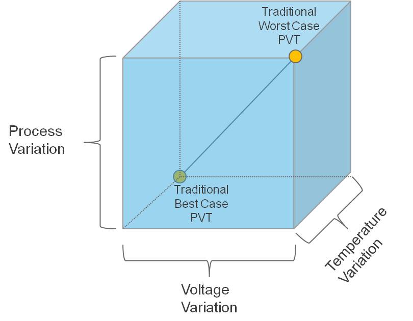
Typical timing analysis consists of examining the operation of the design across a range of process, voltage, and temperature conditions. In the past it was acceptable to expect that the operational space of a design could be bounded by analyzing the design at two different points. The first point was chosen by taking the worst-case condition for all three operating condition parameters (process, voltage, temperature) and the second point was chosen by taking the best-case conditions for the same three parameters.

Figure 1 – Operating Conditions Domain for Timing Signoff
As shown in Figure 1, we assumed that the worst slack for a design in our three-dimensional box was covered by just two points because delay was typically monotonic along the axis between the points. And since delay at earlier process nodes was dominated by cell delay, there was little thought to looking at the process range for interconnect layers; therefore, parasitic files were typically extracted at the nominal process.
When process nodes moved to lower geometries like 65nm and 45nm, supply voltage levels were reduced to 1.0 volt or less and thus temperature began to have a contrarian effect on cell delay. Whereas in previous technology nodes delay increased with high temperature, temperature inversion effects began to increase delay at lower temperatures under worst- case voltage and process conditions. The direct result to timing signoff was an increase in the number of corners for signoff and optimization. The number of operating corners quickly doubled from two to four, or even five for those who insisted on timing test modes at typical operating conditions.
As routing pitch began to decrease so did the amount of coupling capacitance that was seen, and with it the crosstalk delay effect. Process variations in metallization now had a non-negligible impact on the timing of the design. Plus, metal line width became small enough to impact the resistance of the wire with just a small amount of variation. Given that metallization is a separate process from base layer processing, engineers could not assume that process variation tracked in the same direction for both base and metal layers. Therefore, at 45nm and to a larger extent at 28nm, multiple extraction corners were now required for timing analysis and optimization. These extraction corners consisted of worst C, worst RC, best C, best RC, and typical.
Summarizing the situation at 28nm, we have the following corners:
- Temperature: Tmax/Tmin
- Process (base layer): Fast-Fast, Fast-Slow, Slow-Fast, Slow-Slow, Typical
- Process (metal): Cmax, Cmin, Typical, RCmax, RCmin
- Voltage: Vmin, Vmax
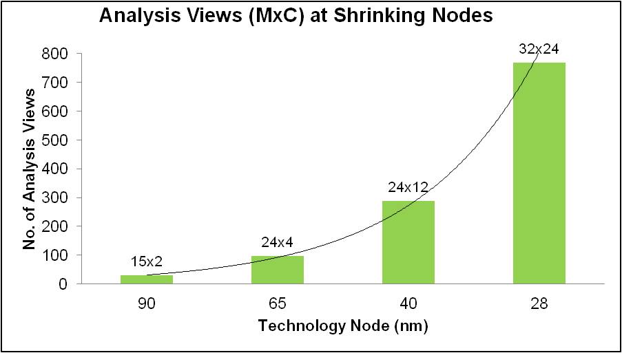
If you wanted to exhaust the number of combinations for analysis you’d have 2x5x5x2 = 100 corners. If this isn’t realistic, then what is a good reduced set? Let’s reduce the base layer process corners down to only best and worst cases and eliminate ”typical” from our metal layer process. This reduces our overall corner count to 2x2x4x2 = 32.
Then let’s assume for a given design that we have three test modes and five functional modes. Those eight total modes result in more than 250 views to be analyzed. This is still a number that for most companies is unmanageable, so we further whittle this down by hand-waving and making assumptions (hoping) that certain combinations of conditions either won’t happen or will be covered by other operating configurations (in particular, test modes at extreme voltage and temperature).
After all the hand-wringing and engineering justification has been exercised, you might get the number of views down to about 100 or less depending on your tolerance for risk. For metal re-spins or minor design revisions, the risk of failure may be low—but for new designs that can define the success of your company, you are going to analyze every combination.

Figure 2 – Increasing Timing Views for Advanced Process Nodes
At the 20nm process node things become even more complicated due to double-patterning technology (DPT). Because lithography limitations require two masks for the same layer, the masks must be precisely aligned such that the spacing between patterns is consistent across the die. Unfortunately, there will always be some phase shift in the masks relative to each other and it may not be possible to predict what that phase shift is, which results in more variation. One way to handle that is by extracting more corners to simulate the bounds of the shift. The end result is a possible doubling of the corners going from 28nm to 20nm. Even if you doubt the number of timing analyses required at 28nm, it isn’t going to get any better at 20nm. It’s just going to get worse.
Analysis is Only Half of the Story
So far we’ve discussed the reasons for an exploding number of corners required to verify a design for timing. Those reasons are driven by lower rail voltages, variations in the process of metal layers, and variations due to new lithography techniques that are required to process patterns at 20nm and below. Once we’ve found a way to get over the mountain of timing analyses, it would seem our problems are solved. Absolutely not. We’ve just hit the tip of the iceberg.
Processing the results and fixing timing violations is where the real work begins. The first challenge is in presenting a consolidated view of the design to the timing optimizer. When analysis involves more than 100 different views, the consolidation of the results becomes critical in terms of data management and capacity.
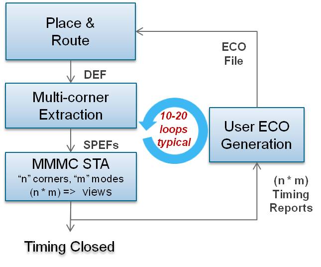
Many customers today have their own home-brewed scripts to deal with managing the results from different views. Figure 3 shows a typical flow where designers insert their own optimization utility to close the design. These utilities range from simple consolidation of native tool reports to complex customized construction of timing and slack reports utilizing exported timing attributes. For scripts that simply merge reports, the resulting data can be more than an implementation style tool can handle.
Today, most tools that manage timing optimization generally operate on a subset of the views needed for signoff due to capacity limitations. There are complex solutions that can parse timing attributes into more efficient representations of the design timing, but the overhead of maintenance and the expertise required may be beyond the reach of the average engineer.

Figure 3 – Typical Signoff Closure Flow
The second complication to optimization is an old problem that continues to frustrate engineers today. That is the miscorrelation between implementation timing and signoff timing. The only alternative to mitigating this problem is by margining the design during the implementation phase so as not to incur violations during signoff timing. With power being one of the most critical design metrics today, adding excessive gates to ensure minimal violations at signoff is a poor tradeoff that leads to power-hungry designs, more area, and fewer chips per wafer.
The iterations required to close timing differences between implementation and signoff timing are further complicated by the fact that signoff timers are not physically aware. Placement of inserted buffers is left to the implementation environment as a post-processing step for engineering change order (ECO) generation. Often the placement of new cells is dramatically different from what is assumed by the optimization algorithms due to the placement of existing cells and lack of vacant space in highly utilized designs. This results in a significant mismatch between the assumed interconnect parasitics during optimization and the actual placement and routing of the ECO.
Figure 4 shows the potential uncertainty involved in cell placement that affects assumptions made in a traditional signoff ECO flow. In this figure, both Case 1 and Case 2 result in added uncertainty to the final timing result. However, Case 1 is much worse because it impacts the timing of paths that may have already met timing. Not only is the impact on timing unknown, but it is also impossible to tell which paths will be affected by the movement of cells to legalize placement. What previously may have been a timing-clean view (mode, corner combination) could potentially have many violations after routing and placement legalization of the inserted cells.

Figure 4 – Consequence of Non-Physically?Aware Signoff ECO
Addressing the Gaps in Today’s Signoff ECO Flows
We’ve examined some of the factors that have increased the complexity of timing signoff and design closure. An increasing number of analysis views and differences between implementation and signoff timers have created numerous obstacles to creating a design that is timing “clean.” The biggest issues are:
- An exploding number of analysis runs that need to be performed at 28nm and below
- Runtime of both parasitic extraction and timing analysis
- The ability of EDA tools to look across hundreds of views during timing optimization
- Timing miscorrelation between implementation and signoff
- The lack of physical awareness when performing timing optimization and ECO generation
Let’s look at some ways to mitigate or eliminate some of these problems.
Increased analysis runs
For an exhaustive analysis, the timing analysis engineer must run every mode-corner combination. The quickest way to arrive at a consolidated answer is to distribute the mode-corner combinations across a compute farm and run them in parallel. There may be some opportunity to bound some operating corners by focusing on extreme corners, but with temperature inversion affecting cell delays, and with phase mask shift uncertainty at 20nm, you can never be sure that the corners have caught all violating paths between the expected best-case and worst-case conditions. Today, exhaustive analysis is the safest approach to ensure that a design works under all possible operational conditions.
Tool runtime
Once you have distributed all of your views to individual servers, the bottleneck becomes the pure processing time required for a single view. Timing analysis and parasitic extraction tools must be architected to leverage multi-core processing. Today’s timing analysis tools generally scale reasonably well up to four cores and provide practical scalability up to eight. But while portions of the timing flow today can scale beyond eight, the performance speedup beyond eight has a negligible return when considering the overall timing analysis flow.
Scalability with an increasing number of cores is a must-have for analyzing large system-on-chip designs, especially with compute servers containing up to 16 cores. Because scalability is largely dictated by the percentage of processing steps that are multi-threaded, it is not sufficient today to claim that only portions of the timing analysis and extraction flows are threaded. All steps, from reading in the design to reporting or generating output files, must be multi-threaded.
Optimization capacity
Timing optimization, which is typically in the realm of implementation tools, is generally limited in capacity when optimizing over multiple views. Most vendors recommend optimizing a subset of views so as not to exceed the capacity limitations of the tools. When optimizing across more than 100 views, it is critical to have the capacity to construct a common timing graph that represents a composite picture of all modes and corners. Reduction must not lead to a loss in accuracy or missed failing endpoints—otherwise the yield of timing fixes becomes poor and approaches negligible benefit.
Implementation versus signoff correlation
It’s clear that miscorrelation between implementation timers and signoff timers is one of the biggest reasons for the number of ECO iterations needed to close a design. Users have gone through great lengths to build custom solutions that leverage timing attributes and reports from signoff timers for the purpose of timing optimization.
Today’s design closure requires the timing optimization engine to operate off of the same timing engine as the signoff tool. In this way “what-if” analysis can be dynamically checked before committing changes to an ECO. Some solutions on the market start with signoff results but lack the integration to perform “what-if” analysis by iterating through the signoff tools. This is an absolute must to reduce iterations and improve the yield of timing fixes.
Physically-aware timing optimization
The last piece of the puzzle, and the most important to achieve timing closure convergence, is the ability to reduce uncertainty that occurs during legalized placement and routing of an implemented ECO. Timing optimization in the signoff area is limited to a logical view of the design, and therefore makes assumptions about the placement of inserted cells that varies radically from the actual physical implementation.
Understanding the location of cells, the vacancies available, and the topology of routes during the optimization process results in design changes that predictably match the reality of design implementation. This capability not only produces better quality ECOs, but also minimizes the impact to paths that already meet timing. Figure 5 illustrates the quality-of-results (QoR) difference between physically-aware and non-physically?aware hold-time optimization and the degradation in setup time that can occur. The value of better quality ECOs also enables the number of ECO loops to be reduced, which can have a huge impact in minimizing the total time to timing signoff.

Figure 5 – QoR Benefit of Physically-Aware Timing Optimization
(Total Negative Slack / Failing Endpoints)
Conclusion
The preceding list of features are all well within the reach of today’s EDA technology. Integrating signoff and implementation tools has been discussed for many years and there have been attempts to make it happen. The key to making it work is to have a system that is built with integration in mind. This includes common timing engines and unified databases so that the exchange of data from implementation to extraction to timing is a seamless process and results are consistent. Patching together long-standing point tools is generally a suboptimal solution that neither delivers on efficiency or runtime performance.
Fortunately for the user, there are timing closure solutions on the market today— such as the Encounter Timing System from Cadence—that address the items listed. Customers should expect their EDA vendors to provide solutions that address today’s signoff timing closure deficiencies in the overall design flow process. Otherwise, with the movement to smaller process nodes, this phase in the design flow could become the longest step to taping out a design.
About the Author: Ruben Molina
 Ruben serves as the Director of Product Marketing for Encounter Timing System at Cadence. In this role he is responsible for setting product rollout strategy, establishing tool requirements based on customer needs, and assessing the competitive landscape in the areas of pricing, licensing models, and technical capabilities.
Prior to joining Cadence, Ruben held marketing director positions at Magma Design Automation and Extreme DA where he was the responsible for directing business development and product marketing for all static timing analysis and parasitic extraction products. In addition to Magma and Extreme DA, he has held senior management and technical positions at LSI Logic in the areas of design methodology. This includes power, crosstalk, clock distribution, delay prediction and variation modeling. He also spent several years as an IC designer for Hughes Aircraft, Radar Systems Group. Ruben holds a BS in Engineering and MSEE from California State University, Los Angeles. He is the co-author of seven U.S. patents


Cadence’s Ruben Molina discussed the challenges of managing the number of modes and corners that must be verified, especially in light of last-minute ECOs. How are you managing this problem now?