

Verification and test have always faced a tricky paradox: How do you build equipment to test and verify the biggest, fastest devices ever created?
After all, it stands to reason that the tester has to be faster than the thing it’s testing, and the prototype has to be bigger than the thing it’s prototyping. It means that those folks have to always be running ahead of the fastest runners in order to handle the problem.
When prototyping large SoC designs, this issue has always been handled by throwing a wall of FPGAs at the problem. Even though this poses significant challenges with issues like design partitioning and mapping the design to an FPGA-friendly format, it has been the most effective method available for getting a usable prototype up and working.
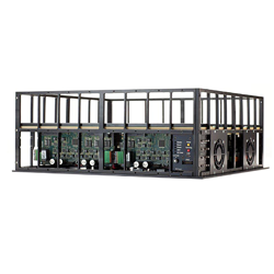
A few years ago, Synopsys acquired FPGA synthesis company Synplicity, and, with that acquisition, they picked up one of the industry’s best and most flexible FPGA prototyping platforms – HAPS. HAPS had itself been acquired by Synplicity just a couple years before that – from Swedish company Hardi. HAPS boasts a flexible architecture that allows multiple FPGA boards to be stacked “like Legos” to build an almost arbitrarily large prototype. You simply plug together the number and type of HAPS boards required to handle your design, and you’re off to the races. The boards connect via what the company calls “HAPSTrack” which provides high-speed connections between the stacked FPGA-based prototyping boards. The vertical orientation makes the FPGA-to-FPGA-on-a-different-board connections much shorter, allowing the prototype to be scaled without significant performance penalties and timing problems.
Synopsys recently announced a major upgrade to HAPS called “HAPS-70”, and a lot of the challenges we’ve been discussing just got a lot easier. Thanks in part to Xilinx’s gi-normous 7-series 3D (not really) FPGAs – aimed specifically at the prototyping market, the number of FPGAs required for the biggest prototypes has dropped significantly. Of course, the size of the biggest designs has increased significantly at the same time, so overall, the industry is doing little more than treading water on the size front.
With HAPS-70, the company claims they’ve increased the speed of those connections by 3x, with a new flavor of time-domain multiplexing and faster connectors. Time-domain multiplexing allows multiple signals to be routed through a single IO channel. Typically, when partitioning a design across multiple FPGAs and across multiple boards, the number and speed of available IO channels becomes a bottleneck. Improving the performance by 3X allows either the speed of the connections or the number of connections to be increased. Combining this with the greater capacity of the new FPGAs, we get a multiplying effect – so we can do much larger designs without increasing the complexity of the partitioning, and still the speed and capacity of the interconnect between partitions improves.
Speaking of partitioning, Synopsys is challenging the norm of manual partitioning of prototypes. For years, even back before Synplicity was acquired by Synopsys, they (Synplicity) offered an automated FPGA partitioning/prototyping synthesis tool called “Certify” that not only automatically partitioned a large design into FPGA-sized chunks, but also handled many of the other tasks for converting an ASIC/SoC design into something that could run on multiple FPGAs. While Certify has had a steady cult following over the years, there was also a sizeable chunk of the market that didn’t believe in automated partitioning – at least not enough to plunk down the cash for a copy of Certify. Synopsys says that the automated partitioning capabilities have improved significantly over the years. Perhaps this is the time we should all give automation another shot? If it works for you, it will have a major impact on your productivity in getting your prototype up and running. Even if you do partitioning manually or partly-manually, Certify brings some very handy capabilities to the table in mapping a design not intended for FPGA use into an FPGA prototype. Synopsys claims a productivity boost of up to 10x for users adopting Certify for their FPGA prototyping.
Another common issue with FPGA prototypes is the limited amount of trace data we can save and the resulting limited amount of debug visibility we get into our design. With HAPS-70, Synopsys has solved this by allowing the use of external memory for trace storage. In the past, trace data was stored in block RAM on the FPGAs. This sounds great in theory – it is fast and doesn’t use up precious IO space. However, the design itself often monopolized block RAM, leaving a very small sandbox for trace capture. Synopsys says that enabling external storage of trace data gives a 100x improvement in visibility. This can also translate into far fewer spins re-compiling your design to get visibility into where particular bugs are hiding.
Finally, by adopting the new, huge, Xilinx Virtex-7 devices, HAPS-70 brings a significant capacity boost. The system now supports from 12 to 144 million ASIC gates with a fully-populated rack. That’s a lot of capacity – probably plenty for most current-generation IC design projects. There is a performance boost as well, and, combining that with the faster connections supplied by HAPS, you’ll probably find yourself with a much faster prototype. When using prototypes to develop real-time software or other performance-critical applications, this can be a huge benefit.
If you’re using your prototype as a hybrid or as the hardware accelerator for traditional simulation, you’ll get a performance boost from the new 400MB/s UMRBus. This allows external processes to communicate much faster with your hardware prototype.
Finally, Synopsys has put a good deal of effort into making the software that goes with HAPS be “HAPS-Aware”. This means that, although the software can handle and target a variety of prototyping platforms – including those you build yourself, you’ll get more robust support for HAPS because the software knows a lot about the HAPS platform that can make your life easier. The software can validate many aspects of the prototype, so that when you run into a problem, it’s more likely a problem with your design itself than with the prototyping system. The software validates that your boards are plugged in correctly and that boards and daughter cards are in the correct connectors. It also can validate the clock configuration and the UMRBus link to your host system. Having all these potential problems off the table means that you can get to work using your prototype faster, rather than spending your time getting the prototype itself set up and working.
Altogether, these improvements make a much more compelling argument for HAPS. Synopsys, like other prototyping companies, tells us that the biggest competition for these systems is home-grown prototypes. With the size and complexity of modern designs and the FPGAs that can prototype them, however, it is becoming more and more questionable as to the value and wisdom of making your own prototype versus using a commercially-available off-the-shelf system like HAPS.


There has been a lot of action in the FPGA-based prototyping world lately. The latest is Synopsys upgrade to their HAPS line. What do you think?