


This is a tale of two memories, and it is brought to you by the number 4.
These two memories don’t necessarily know each other, although they might reside near each other and might even have occasion to talk to each other. But, by and large, they have different stories to tell, which we will take in order.
OK, so perhaps this is two tales of two memories.
Once is never enough
The first is a deceptively simple-sounding tale. It is Kilopass’s reduction in footprint of a non-volatile memory (NVM) one-time-programmable (OTP) cell by 4x. Oversimplified, this is done by removing one of two transistors from a more traditional two-transistor (2T) cell.
Such older 2T cells use one transistor as a “select” transistor to isolate the cell for reading or programming. The other transistor has the oxide that either remains intact or gets shorted when the cell is programmed. That’s been a pretty traditional configuration for a long time.
Problem is, of course, that it requires two transistors. Quick (and, as it turns out, inaccurate) math would suggest you could cut the area consumed in half if you eliminated one of the transistors. There have been attempts at 1T cells before – even fractious ones. But those involve a non-standard transistor whose gate oxide has two parts with different thicknesses; some design rules are bent to make this happen.
It’s important to remember that the folks who use these things are designers or architects embedding memory in an SoC. In other words, we’re not talking entire chips made of these cells, sold at mega-volumes. If that were the case, you could tailor the process any way you wanted in order to optimize the memory. But because this has to play nicely with other logic and processors and who knows what else, it’s going to be made out of “standard” CMOS.
So this has left memory users with two choices: a 2T cell that’s fully CMOS compliant or a 1T cell (Kilopass calls theirs a 1TH cell) that can be made only by violating some standard DRCs. That’s messy. (Or messier.)
So what’s changed now?
Kilopass is using a different approach to the 1T cell. It uses only a single gate oxide, so from that standpoint, it’s standard CMOS. But they do require one additional step to the process – one they say is relatively easy and non-critical (in terms of feature size… it’s critical in the sense that, if you omit it, it won’t work… but you knew that).
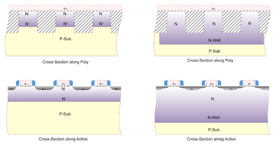
Each of the transistors is effectively a PNP whose emitter connects or doesn’t connect to a word line, depending on whether the antifuse is intact (making it a capacitor) or blown (making it a resistor). Normally a PNP would involve an n-well sunk into a p background. And if you want all of the n-wells isolated from each other, well, you’d use some kind of isolation like p wells or oxide or something. Which takes up space. If you’re going to have a big array of these things, you want to pack them as close together as possible.
One way to save space is to sink all the n-wells into a single large p substrate. But the typical implant drives in deeper than the shallow-trench isolation (STI) that separates rows of transistors. That means that all the cells are effectively shorted together. You want the cells that share a bit line to share a connection, but you don’t want to short all the bit lines together.
So what they’ve done is added a special implant step that creates an n-well that’s shallower than the standard one. This keeps the bottom of the n-well above the bottom of the STI, isolating the bit lines from each other. You can see this in the figure below (where the right side shows what a standard configuration would do, with the n-well connecting everything, and the left side shows the new shallower n-wells protected by the hashed STI). This one extra implant mask is what is needed above and beyond the standard process; what you get for your efforts if you do that is not half the area, but the area divided by 4.
They’re also targeting this for use as a many-time-programmable (MTP) (or perhaps few-time-programmable or FTP) memory. Which might have you wondering whether they’ve found a way to reliably heal the blown antifuse into a nice clean oxide capacitor again.
The answer is, of course, “No, they haven’t.” Because the cell is so small, they can oversupply the cells, creating enough redundancy that, if you want to reprogram some cells, you don’t reprogram the cells you used before; you simply program some new cells and replace the old ones with the new ones. Obviously, you can do that only so many times before you run out of extra cells (leading to the question of whether it’s “many” or “few”), but it does give a level of flexibility that would not otherwise be possible with an OTP cell.
Al Gore Rhythm
Our second tale involves a cell that couldn’t be more different. An OTP cell is as permanent as is physically possible. Our next cell is a DRAM cell, a type of memory that’s not just volatile, but is so volatile that it has to be refreshed even when the power stays on. It’s the complete opposite of an OTP cell on the “permanence” axis.
This story is about getting memory out of the way of computing performance. A processor may churn away on knotty problems, but if it needs to wait for memory, everything comes to a halt. And memory is a notoriously serial problem. If you need 12 words from memory, then they pretty much go into a queue. Yes, a smart memory manager can reorder the requests to take advantage of things that are in the same fetch, but the chances are that something is going to have to wait.
Caches have helped to reduce the number of times that this happens, but if you get a cache miss, you’re back in line, hat in hand, waiting for data. Multi-port memories can help, but then you have to physically build all those ports, and, depending on read and write sequences, you could still get blocked.
So a company called Memoir has been working on what they call “algorithmic memory” to improve memory performance, in terms of memory operations per second (MOPS) by – you guessed it – 4x. And in trying to understand how they do this, you end up wading into rather murky waters where the answer is, “It depends.”
They talk about a mixture of techniques like caching, buffering, virtualization, data encoding, and pipelining. And a design tool that takes your memory access requirements, examines around 10,000 different possible design alternatives, and returns to you a correct-by-construction architecture that will deliver the promised performance – with a single physical port. That all sounds nice, but what does it really mean?
I had a conversation with Sundar Iyer, Memoir’s co-founder and CTO, and he took me through some basic scenarios. It starts with, of all things, error correction coding. Which seems to be finding its way into various things that aren’t actual error correction (like PUFs). Let’s walk through it.
Say that you want to be able to do two reads simultaneously through a single port. A completely brute-force approach would have the entire memory duplicated on two blocks. Huge overkill. But… let’s say you broke the memory into four different blocks. Now you’ve reduced the chances that both reads will come from the same block; if the addresses of two requested words are far enough apart, you can stage two reads on two blocks and get the results more or less simultaneously.
But, of course, you can’t rely on the two reads being in different blocks. If they’re from the same block, then one read would still be blocked until the other is done. But rather than storing a duplicate version (as in the overkill suggestion above), you could have an extra memory block where you store an encoded version of all the data.
Here’s one way you could do it (making something up): when writing data into a particular address in one of the four internal memory blocks, additionally combine all of the four entries at that address in all four blocks using an error-correction scheme. Which requires extra bits of redundancy but is far more efficient than simply replicating data.
Here’s how it works: Let’s say you use an encryption code that can correct 8-bit errors, with each memory block being 8 bits wide. So now, if you have two reads into the same block, you can do the first read from its actual memory block; for the second read, you go to the encoded data. You read that address, presenting data from the three unblocked memory blocks; the system can then treat it as corrupted data, with 8 bits missing (the 8 bits that we can’t get because we’re blocked), and reconstruct the missing 8 bits. So while we read the first byte straight out of memory, we reconstruct the other byte from the encoded side-store.
Of course, you can say, “That’s all fine and good, but what if you are reading three bytes, two of which come from two different memory blocks, and the third of which comes from one of those same two blocks – in other words, the third byte is now blocked?” Our prior scheme no longer works because the encoded data was set to reconstruct only 8 missing bits. Now, because two of the memory blocks are in use, we’re missing 16 bits, 8 of which we want.
If this is one of the access patterns needed for the design, then the four-block 8-bit correction wouldn’t be used. Instead, you’d design with 16-bit correction and you might use more than four blocks. When you start thinking through the various access patterns, you can start to see how there are many different ways to approach this. And all we’ve looked at is the data encoding. Add the various other schemes they use – load-sharing, caching, etc., and you get a sense of why there may be thousands of different possible ways of assembling the memory.
The key, though, is that you design the entire system with specific applications and access patterns in mind, and the “memory compiler” generates an architecture optimized for that application. It may not be optimized for other applications, so this clearly is better suited to embedded designs, where you know what you’ll be dealing with (or at least you think you do). Wouldn’t work so well for a desktop computer, where you have no idea what’s going into the memory.
And I should clarify that the scenario I presented was but one overly-simplified way to address the problem for illustrative purposes, and it probably isn’t used exactly as I described in any real design.
So there you have it. One memory cell that’s 4x smaller; the other memory providing 4x the performance.
Which is why today’s piece was brought to you by the number 4.
[Cue Toots Thielemans]
More info:


New goings on in the memory world. What do you think? Useful stuff?