

There has always been a class of designers for whom the biggest is just not big enough.
Despite over two decades of Moore’s-Law-driven progress in FPGA design, with exponential growth in gate counts tracking at or ahead of the rest of the semiconductor industry, there have always been (and still are today) those folks who want bigger and better FPGAs than the best the industry could deliver. Ten years ago, when Xilinx introduced the first Virtex devices (with a whopping 27,648 logic cells in the biggest device), these people said, “27K just isn’t enough. Give us more.” Two years ago, when Virtex-6 rolled out with a staggering 760,000 logic cells, (a growth of about 30x in less than a decade) the same users were still not impressed. “OK, I guess we could get by with four of those.”
You’d think the day would come when these folks would say, “There, that does it. Finally, you made one big enough.”
Nope.
Xilinx announced this week that they are now shipping Virtex-7 V2000T devices with, as you can probably guess from the part number, two million logic elements. Utilizing their revolutionary “2.5D stacked silicon interconnect technology,” the company is now shipping the world’s largest FPGAs, and probably the largest logic devices, ever made. With a claimed 6.8 billion transistors (we didn’t actually count them), that would make them more than double the size of anything announced to date by competitors. Xilinx is also claiming that the new stacked silicon approach gives them “More than Moore” growth – putting them ahead of the already breathtaking pace of the semiconductor density explosion.
Let’s do a quick little marketing fact check and see if that adds up. The original Virtex family had, as we just mentioned, 27K logic elements. It was based on .22 micron technology (which, in today’s parlance, would be 220nm). If we walk that through the process nodes since then – 180nm, 130nm, 90nm, 65nm, 40/45nm, 28nm – with a simple 2x at each stop, 28nm should be giving us 1728K logic elements. At 2000K logic elements, they are indeed ahead. If we look at years vs. process nodes, the company has jumped six nodes in a decade. How you rate their performance there depends on whether you use the “2 years” or the “18 months” version of Moore’s Law. One more interesting check might be what a “logic element” is. Back in the old days, a logic element was a four-input look-up table (LUT4). Today, LUTs are wider so FPGA companies do an “equivalence” back to the number of LUT4s that their current technology represents. The math basically works out, but you won’t actually find 2 million of anything on your V2000T device. What you will find are 305,400 “slices”, where each slice contains four 6-input LUTs and 8 flip flops. Xilinx reckons that gives you about two million LUT4s worth of “stuff”.
No matter how you market it, that’s a lot of logic. Not shown in this picture are massive increases in the amount of non-LUT technology on the FPGA, like 2,100 DSP48 slices, 36 multi-gigabit serial transceivers (rated at 12.5Gbps), and 21Mbits of RAM. Altogether – 6.8 billion transistors worth of goodies.
There are two interesting aspects to consider about this beast: how Xilinx achieved this result and what it means to the gate-crazed fanatics who will be designing with it.
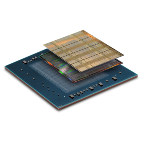
Xilinx got a two million LUT device by stitching together four smaller FPGA slices using a silicon interposer. Wait, isn’t that cheating? You bet it is. And it’s kinda’ awesome. For years, people who have needed more capacity than the largest FPGA can deliver have been building boards with several of the largest FPGAs. Prototyping boards often have four, eight, or sometimes even more of the largest available FPGAs, connected by their IOs. Of course, the number of IOs is limited, so multi-FPGA designs had to be partitioned carefully to avoid overloading the available channels between them. Connecting big FPGAs through the IOs also causes issues with power consumption and speed.
Xilinx’s 2.5D stacked silicon interconnect solves these problems and gives us a host of new, game-changing side effects to boot. Here’s how it works: The smaller FPGA chips are stacked side-by-side onto a silicon “interposer” chip – connected by tiny “microbumps”. This allows on the order of 10,000 connections to be made between FPGA chips – far more than could be achieved using conventional IOs. Furthermore, the speed and power profiles of routes through the interposer are much closer to pure silicon routes than those that go through IO buffers, onto PCBs, and back again into another FPGA. Xilinx trained their place-and-route tools to map connections through the interposer in just the same way it does normal on-chip routes. The result is that we can do our designs for the V2000T just the same as we would for a normal, two-million gate, monolithic FPGA – except for the fact that none of those exist.
The obvious tradeoff here is about yield. Building a monolithic part this large would require an enormous die – sending yields plummeting to unacceptable levels. Building the big part from four smaller parts plus an interposer increases the complexity of some parts of the production process but requires much smaller successful dies, increasing effective yields and lowering costs. Xilinx claims that this gives them about a 2x effective density advantage at any given process node.
While that’s cool, that’s also the boring and expected part. The really exciting potential comes when one starts to realize that the chips being stitched together on the silicon interposer don’t have to be all from the same wafer – or even on the same process. Why is this important? The best process for doing something like multi-gigabit transceivers might not be the same as the best process for FPGA fabric, or memory, or analog, or…. You get the idea. One could visualize stitching together a bunch of diverse chips – each with its own optimized process – into a super-SoC that would outperform anything that could be built with a monolithic die. Imagine a device with slices of FPGA fabric, large chunks of memory, non-volatile or flash slices, optimized embedded processing blocks, and high-speed IO slices – all integrated onto a single interposer and acting as one giant chip.
In a more conservative but similarly interesting vein, Xilinx hinted at binning slices and mixing-and-matching differently-binned slices on each device. This suggests that a device might contain some mixture of “fast” slices and some that have lower leakage current. Properly used by the tools, this would allow performance-critical blocks to take advantage of the fast fabric and overall leakage to be reduced by the presence of the slower, less leaky ones. It isn’t clear the degree to which Xilinx is taking advantage of this technique – and how much support exists in the current tools to really gain leverage from this architecture.
Today, however, we get just a tiny view into that future. Xilinx was able to coalesce elements of a perfect storm of process technology to pull off their current feat. The FPGA slices are remarkably consistent and regular – making the interposer design straightforward and efficient. When you’re attempting a new trick, it’s nice to control as many variables as possible. That’s exactly what Xilinx has done here. They announced about a year ago that this 2.5D technology would be shipping “in about a year”. One year later – they’ve got devices in customers’ hands, devices running public demos, and devices being passed around for us editors to poke with our ink-stained fingers. They’re real. Delivering on such a complex new process – with so many potential points of failure – is a remarkable operational achievement.
For those power users that need all the gates they can get – the benefits of the larger device versus partitioning across multiple FPGAs are substantial. According to Xilinx, the performance is significantly better, the power consumption is 1/7 what it would be connecting discrete devices with IOs, and the design time is dramatically reduced due to the elimination of the partitioning step.
Xilinx thinks that the markets for this new device include ASIC replacement (people putting large designs that would previously have required ASICs into FPGAs), Extending integrated systems (in areas like wired and wireless communications, storage, military, and video processing), and ASIC/ASSP/SoC prototyping and emulation. All of these domains share the need for as many gates as current semiconductor processes allow.
Xilinx calmly waved their collective hands and said that the tools required to back up this process were a simple extension of their existing tool suite. Clearly they were not. Handling the massive designs required to fill a two-million LUT FPGA requires a big boost in throughput for synthesis and place-and-route tools. Also, managing the transitions through the interposer must pose some substantial challenges for placement and routing. Finally, enabling proper team design capability – which is a must-have for designs this size – could involve significant re-work to the tools. Xilinx has a massive number of engineers working on design tools and IP. It’s likely they’ve all been pretty busy behind the scenes getting to the point where these huge devices could be realistically supported. The company claims that the complete design environment supporting these new devices is ready and in use today at key customer sites.
One question that might come up is the reliability and robustness of stacked silicon compared with monolithic devices. Without giving meaningful detail, Xilinx claims that reliability should be very high. They make arguments like the microbump technology being proven previously in a number of other areas, and that considerations like thermal expansion are mitigated because the stack is silicon-on-silicon. Thermally, since the design is still basically planar – without active-on-active stacks, the heat dissipation properties are not likely to be significantly different.
The delivery of stacked silicon interconnect in a production FPGA is an important milestone in what promises to be an exciting journey. While this first effort delivers primarily evolutionary advantages – greater capacity, lower power consumption, higher speed – that amount to about one process node worth of gain, long-term possibilities of stacked silicon are much more revolutionary. The ability to mix heterogeneous dies in a single device with massive, low-loss interconnect could change the long-held rules of semiconductor design. It’ll be fun to see where it goes.


“You’d think the day would come when these folks would say, “There, that does it. Finally, you made one big enough.”
Nope.”
I don’t know why you would think that there could ever be enough gates in one FPGA to satisfy anyone designing ASIC’s on the same process node. Because the ASIC and FPGA use the same process, and the FPGA necessarily has the overhead of run-time reprogrammability, the FPGA cannot possibly keep up with the requirements of the ASIC developer without using significantly more silicon area. Xilinx will not doubt continue the stacked silicon approach to meet these needs for process nodes yet to come.
You caught me Gabor. I agree with you completely. As long as people are designing ASICs on the current process node (whatever that is) FPGAs will not be big enough for their prototyping needs.
Today, FPGAs are at least a node ahead of most ASICs. We are talking about FPGA devices here shipping on the 28nm process node. Not many ASICs being shipped today at that density. Combined with the advantages of this 2.5D packaging technology, FPGAs are actually even closer to the density of an ASIC, but still behind, I’d say. I think there is at least a 10x overhead required for the programmable fabric parts.
It did make a more interesting sounding intro to the article the other way, though.