

Hoover Dam is pretty damn impressive. Why, some might simply say it’s a pretty dam.
As you take the tour, much is said about its size, the effort to build it, the clever techniques used to cool the concrete, and, if you’re lucky, the volume of water rumbling through the penstocks inches below the ominously vibrating surface you’re standing on.
But even before you get to the tour, there’s another inescapable feature. Assuming you park at the south end and walk back towards the dam, you have to pass by a monstrous gaping maw that seems like a portal into the belly of Hades itself.
It’s the overflow sluiceway, and it’s so huge that you could easily put a car down it (at least that’s how I recall it). And you can’t see the end – it just curves steeply, smoothly down into utter blackness. Frankly, I find it the most impressive feature there (so much so that it yielded a scene in a nightmare many years ago).
Of course, its purpose has nothing to do with some dark horror film; it’s simply the relief valve for when the lake gets too high. (Assuming the Colorado River weren’t so oversubscribed that it might actually get too full…) It would be no good at all if rising water simply topped over the dam; that’s considered rather poor form. So, just before the water reaches the level at which it could cause some actual damage, it spills over and out through the sluice, harmlessly passing through the void to rocket across the canyon further downstream.
The design of this isn’t necessarily trivial. You wouldn’t want, for example, just to dig out a dirt sluiceway. If you did, then, when it was used, the dirt would erode away in all kinds of nasty, unpredictable ways – the spillover event would be destructive, and you’d have lots of work to do to get things shipshape again.
Which is why the thing is lined in concrete. Water can wash over it again and again with little wear to show for it.
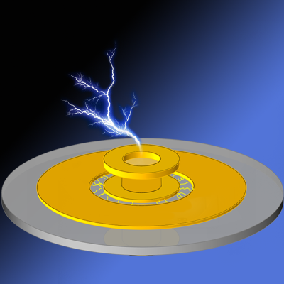
This whole idea of non-destructively shunting some excess to avoid some other damage works not only at this huge mega-scale, but also at the nano-scale. Against random little sparks that might apply brief loads on your circuits that go orders of magnitude beyond your intended operating range.
Whence those sparks? Well, that’s not at all a trivial question. I remember heated debates years ago about whether the electro-static discharge (ESD) spec should follow the “human body” model or the “machine” model. Of course, the manufacturers wanted to use the one that yielded best; the consumers wanted the most rigorous one.
But that debate gets to the essence of the question: exactly what are we protecting ourselves from? In the case of individual chips, it might be people carrying around chips in a manner that is less than ESD-safe or, these days, with increased automation, charge picked up as chips slide along machinery during handling. Those specs were also once considered satisfactory for ESD that might occur in-system. (I recall rumors floating around that the original Macintosh was experiencing issues due to ESD failures on HAL devices inside…)
But, these days, systems far more sophisticated than the original PC are floating around in your pocket and bouncing around in your car. So an entirely different ESD model is used now at the system level. Whereas ESD protection in chips might guard against 2000-V zaps, systems now need to be protected against an 8000-V jolt from a direct contact or a 15,000-V goose through the air – that’s roughly a 1.5-cm spark.
Left on their own, those little ESD circuits on your chip will be toast.
Which means it’s up to the board to handle the heavy loads. Which means figuring out where on the board things might turn ugly and then judiciously laying down surge suppressors of various kinds, generically called TVSs (transient voltage suppressors, not to be confused with TSVs). Big Zener diodes and their ilk.
Using conventional approaches, each of these TVSs must be manually placed. Generally, the system designer will figure out where the vulnerable bits are and protect them. Then you test the board and figure out where the bits you missed are, and you protect them. Not your ideal design approach, and, with potentially hundreds of these things on a board, not your ideal space-saving or low-cost approach.
At least that’s how it’s described by a company trying to change this whole picture. The company is called… wait for it… Shocking Technologies. With a dramatically new technology they call… wait for it… XStatic. (Punsters – OK, guilty as charged – might suspect this name has been around for decades or longer, just waiting for a technology to apply it to… if you’re part of the 80% of the populace that detests puns, then tread lightly here…)
A layer of protection
The approach here is entirely different. Rather than placing suppressors as components on the board, suppression is integrated directly into the board. A separate polymer layer of the XStatic material is placed right between a copper layer with ground connections and the core board material.
The substance is a carefully-concocted nanoparticle cocktail that acts as a VSDM – a voltage-switchable dielectric material. Under normal conditions, it’s simply more insulation. But, at a controlled voltage, it can break down and conduct – reversibly. So once the voltage drops again, it goes back to being an insulator. There’s no known wear-out mechanism, so you could do this all day long.
The key to making this work is in having signals spaced very close to ground. Typically this happens on a “split ground plane,” where the plane has lots of ground shared with signals. Normally those signals are given ample space from the ground, but in critical locations, that spacing can be narrowed to a critical 65-µm gap. If a signal that needs protecting isn’t on the ground plane, it may need to be brought there via a via.
Figure 1. The widened metal creates narrow gaps, where the shunting occurs
When a high voltage is experienced across that gap, the XStatic material under the gap (and only under the gap) becomes conductive, shunting the energy from the signal to ground. They claim to be able to protect against 30-kV sparks.
The material itself is provided in two forms. It can be provided pre-layered onto copper, so that affixing the copper layer to the board (gray-side down, people) automatically installs the extra layer. Or it can come layered on core material as a copper-XStatic-pre-preg-copper sandwich. Shocking Technologies themselves make only the goo for application to copper or core; they have someone else do the application.
The XStatic layer is 25 µm thick – actually thicker than the metal, which tends to be in the 12-18-µm range. If there is any concern about added board thickness, then the pre-preg core can be thinned slightly to compensate.
I got a tour of their plant, hard against the sere southeast San Jose hills. They do their manufacturing locally and have no plans (or need) to go elsewhere. That might sound good for jobs, except for the fact that it is high automation – and not much need for people – that allows them to stay local. So less good for jobs. Regardless, this is where they mix batches out of… stuff… highly-guarded ingredients nestled into an epoxy base.
There are metallic nano-particles in the mix, which are heavy and therefore have a tendency to settle. So a minimum of 24 hours of ultrasonic mixing is required – for some reason, conching chocolate comes to mind – to keep it from settling; much of the energy used goes in cooling the frictional heat that builds up during the agitation. And there is a shelf life of sorts – if it sits too long (measured in weeks) it can settle (although another round of mixing will fix that).
They do a new lot every couple days. Each batch is sampled and tested, both electrically and environmentally. Small boards are made from each lot (they have an arrangement with Sanmina, where they were originally incubated), and those boards are run through tests using the IEC ESD models to confirm that the material works as promised. They also have to pay attention to the glass temperature to ensure that the layer can endure lead-free soldering temperatures.
Tools instead of trial-and-error
They’re planning to take the guesswork out of figuring out just where to place protection. With a tool that will be launched in a couple of weeks, they can simulate every net in the circuit to decide which ones need protection where. This is somewhat tricky, since they have to pay close attention to impedances. The shunt impedance must be much lower than any other impedance so that it gets the lion’s share of the energy.
The tool may also identify places where a signal needs to be routed up to a ground plane, with a break in the ground plane being created, so that protection can be added. This can be done in conjunction with that normal board design, which also allows such standard concerns as ground impedance and return paths to be considered. When released, the routing constraints identified by the tool will need to be manually implemented in the place-and-route tool, but they’re working towards tighter integration in the future.
Their experience is that 2-3 hours allow a complete analysis that will typically identify hundreds more locations that need protection than an engineer might have identified manually. The good news is that, routing aside, it costs no more to add the extra protection, since the entire circuit is underlain by XStatic.
They claim to be able to protect more thoroughly than would be possible using the standard trial-and-error method. They identify three different risks: outright failure, latent failures (“walking wounded”), and latch-up failures. Of the three, the first two are destructive; the last is reversible once power is removed. Their approach is supposed to help to mitigate all three, while a zap-and-fix methodology would handle only the first one.
This business model for this stuff gets a bit more complicated. Assembly houses are conservative bastions – if it works, don’t touch it. So Shocking Technologies’s approach – pre-affixing the material to copper, for instance – is entirely geared to “touching” as little as possible and keeping things flowing smoothly.
Assembly houses are also about reducing any costs. Pennies matter. So adding new materials tends to be a hard sell. Which is why they don’t sell to the fabs: they sell to the OEM manufacturer, who then, hopefully, specifies what it wants to the fab, and the fab complies. It’s a value discussion for the OEM instead of a cost-plus discussion at the fab.
Shocking Technologies (I keep wanting to abbreviate it ST, but another ST might not approve…) estimates costs of ESD suppression today at about 2¢ per line, for a total of $1.50-$2.00 for a cellphone. They claim their solution to be less than $1.50 for that same phone, so it’s cheaper than using components. And covers more nets against higher voltages.
All of that aside, they ultimately get paid very simply: by the square foot of material. All the glitter and glamour of ESD models and EDA tools aside, at the end of the day, it’s a layer of goo on metal. Sophisticated goo, perhaps. But goo nonetheless. Primal, tactile, something you can actually experience on a human scale. Somewhere between our usual nanoscale and scary-sluiceway scale.
But if this sluiceway has no pending nightmare scenarios, it could change how ESD protection is done.
More info:


So, does this look like an ESD panacea or are you skeptical?