

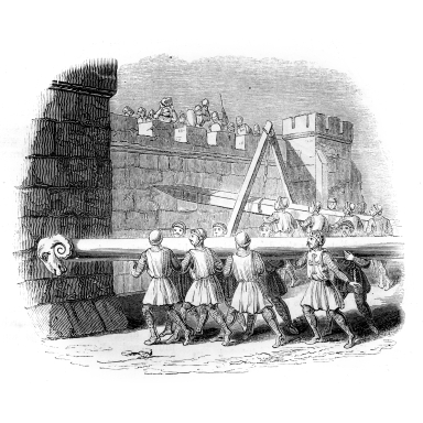
“But melord, the walls on the castle are thick, sir. There be but two ways to breach them, one being through the attaining of prodigious amounts of speed and energy and bounding therewith over the walls, and the other being the attaining of similar energies and smashing through. Both means may, my liege, be considered as unlikely as the migration of coconuts, for the walls be both high and strong. Verily, there may be one more purported way of breaching the wall, but only an the wall be thin enough, whereby one standing on the outside may forthwith find himself standing within the walls with no apparent expenditure of effort, or vice versa. So sayeth your wizard, good sir, mumbling incantations about some infernal tunnel unbeknownst to us all, through which one may pass more effortlessly than passes a needle through the eye of a camel. Such magic as may cause a man to pass through the wall is, however, not welcome in this realm, and the master mason has given assurances upon pain of death that the walls be in all regards of stout enough dimension to thwart any that might attempt to avail themselves of such a tunnel. But he fears, sir, that future castles might be of necessity built with thinner walls, putting the security of the realm in great peril, and foretelling the end of castle-building technology as we know it.”
OK, so quantum discussions amongst the knights of the realm may sound a bit strange. But let’s be honest here: quantum discussions amongst any of us today still sound strange, except that we have managed to convince ourselves that they sound right through the repeated exhortations of our physics professors, who have labored hard, as much to convince themselves as to convince us, that quantum is real. “I do believe in spooky action at a distance! I do believe in spooky action at a distance! I do, I do, I do!”
So let’s put things into more concrete terms. The whole concept of an electric or electronic circuit is predicated on providing places for electrons to flow and, just as importantly, providing places where electrons should not flow. And where they should not flow is through insulators. And in the IC world, we’ve relied on silicon dioxide as an easily-constructed insulator for years. Given such an insulator, there are only three ways to get electrons to violate the sanctity of insulation: give them enough thermal energy to hurdle over the energy barrier; apply a field that causes the oxide itself to rupture; and, if the oxide is thin enough, through quantum tunneling.
The quantum tunneling portion hasn’t really been an issue except when we wanted it to be. The whole concept of Fowler-Nordheim tunneling is that by applying a field across the oxide, one side of the energy barrier is shifted, and what was a uniform thick barrier with a “flat top” becomes more of a parallelogram as one of the sides of the flat top rises above the other. And that parallelogram-like shape gets thinner as you move up, coming to a point at the very top. And through that thinned-out portion, electrons can tunnel (which may create a field that opposes the applied field, leveling out the energy barrier as more electrons travel across).
All neat and tidy. But… alas… in fact, all is not quite so neat and tidy. Insulators can – are you ready for this? – leak. It brings to mind that day of reckoning, that loss of innocence when, rummaging through my father’s dresser drawers, I found, under the Santa suit, a diagram showing that electrolytic capacitors, which we all know can’t sustain a DC current, in fact are modeled with a leakage resistance across them. As I struggled to collect the crumbling shards of my world as they tumbled around me, I realized then and there that I lived in a world far less perfect that what I’d been led to believe. And those imperfections are catching up to us in ways that defy the expectations of the naïve hobbyist or blissfully ignorant engineer.
For, rather than using an applied field to thin the energy barrier and allow tunneling, we have been using the inexorable march of technology to do the selfsame thing. We have been thinning down gate oxides in an endless search for ever more speed, like a tweaker on a rampage. And at some point, resistance falls, and the oxide becomes so thin that electrons can simply tunnel through when they want to. Kind of like that tweaker. Understanding, of course, that ascribing volition to electrons is an anthropomorphic conceit used solely for the purposes of illustration and that, in fact, electrons do not exert free will.
So, cutting through the crap, what this means is that oxides are about to become so thin that they essentially will be porous and provide little insulating power. I have to confess to being somewhat aghast at figuring this out, since it came to me as a byproduct of a discussion on memory cells. I wanted to shout, “Whoa whoa whoa… do you realize what this means?? People, this is HUGE!” As usual I was late to the game, and no one else seemed to share my sense of violation.
OK, so I’m over it. Now what do we do about it? Well, it depends on what we’re using the oxide for. For the vast majority of applications, the oxide should be simply an insulator, separating two conductors that shouldn’t be talking to each other. We’re more or less free to keep those thick. Where we get into trouble is on gate oxides, where we’ve essentially got a capacitor, and we’re trying to increase the coupling to get speed. The obvious way to increase coupling is to thin the oxide, but we’ve run out of runway there. This is where high-κ dielectrics come in. Such materials – including silicon dioxide that’s been monkeyed with – have a higher dielectric constant than pure silicon dioxide and therefore can provide greater coupling for the same thickness. This allows us to use thicker dielectric, staying away from the tunneling regime, while still achieving higher coupling.
It’s ironic that only a few years ago, low-κ dielectrics were all the rage as metal lines got closer and closer together and their interactions could no longer be ignored. In this case, the coupling was undesirable, and so reduced coupling was the goal. So those of us who perhaps weren’t paying as close attention as we should have could be forgiven for tearing our hair out, shouting, “Make up yer mind, fer cryinoutloud, I thought you wanted low-κ, now you say you want high-κ. Sheesh!”
Oxide has also been used to selectively provide a way to transport electrons onto a floating gate as non-volatile memory. As long as independent control of this oxide thickness is available, this can continue. But in logic NVM processes, it’s typically the I/O oxide that is used as a tunneling oxide, and, as the voltages on I/Os drop below 2.5 V, the oxides get too thin. A floating gate where electrons can randomly wander onto and off is pretty much like a prison where people are free to come and go as they choose. It doesn’t really accomplish much. So as you look at the roadmaps of logic NVM folks, they start to get a bit uncertain a couple nodes down the way here. It remains to be seen whether the high-κ solution takes care of the logic NVM needs as well; it’s not obvious that high-κ dielectric is planned for I/O oxide.
So, the bottom line remains that we will indeed be able to continue insulating our circuits. For the time being, anyway. At some future time I’m sure we’ll get back to predicting the imminent demise of CMOS, much as has been done since, oh, 1995 and earlier.


