It’s a lifelong dream for many people to actually fly a plane on their own. The daring, carefree, wind-in-your hair pilot personality, however, is a bit of a myth. In real life, a good pilot is more like a good engineer. You plan and check everything meticulously. You want to find and fix any potential problems before you leave the ground, because once the wheels are up, it’s too late. Imagine you’ve been taking flying lessons now for several months, and you’ve finally logged the training hours, completed all of your exams, and qualified for your first solo cross-country flight. You arrive at the airport, brimming with excitement (and a bit of trepidation). The day is perfect, with crisp, cool air and clear blue skies. You’ve got a lot to do to prepare for this momentous occasion. You spent all night dreaming about the pre-flight planning, walking through every step a hundred times, making sure you didn’t miss a beat. You’re also ready with your pre-flight checklist to verify that your plane is safe to fly, and will perform to expectations when you’re in the air.
When you get to the airport, there’s a bit of a hitch. You’re told that you’ll be performing your pre-flight inspection on a plane “very much like the one you’re going to fly.” “Oh,” they say, “The engine will run slower than the one on your plane, and you’ll see some other minor differences during the pre-flight, but it’s OK.” Then you learn that this testing should provide you with confidence that your plane is good to go. The word “yikes” comes to mind. That is, unless your day job is that of verification engineer who prototypes ASIC designs using FPGAs. Then, it’s pretty much just another day at the office.
After all, that’s what ASIC prototyping is all about. For your pre-flight inspection, you move your ASIC design to a verification environment using multiple FPGAs, and it really does feel pretty familiar, with some notable exceptions (particularly speed, but also memories, clocks, pads). Although you may spend more time in set up than you would for other techniques like hardware emulation, prototyping is much less expensive and gets you a step closer to your real-world application. Once you’ve brought in your ASIC code, partitioned (we’ll get to that…), synthesized your FPGA(s), and loaded them onto your board, you get to actually hook up your stimulus and your output and run it the prototyping version of a pre-flight checklist). Granted, it may look like a slow-motion replay for some applications, but you can see it working.
Tip One: Have a Plan
Wouldn’t it be nice to think that at the beginning of every project, the entire team (yes, entire – the hardware and the software folks in one room, sharing snacks, bottles of water, and whiteboard real estate) would sit down and figure out how best to complete all aspects of the design? After going around the room to share examples of how they document their designs as they go, our team (let’s call them “Utopians for a Better World”) makes a plan for prototyping from the start. Their designs, in addition to being very attractive and efficient, are created with registered known boundaries, allowing you to move swiftly, with effortless joy, among your FPGAs as you prototype. You’re able to minimize your area and maximize your speed. Life is good.
Hey, it could happen. Well, maybe not the documentation part, but to be fair, many teams do consider the issue of prototyping up front. What they decide is another story. Some teams may start prototyping early in the process, while the ASIC design is still in its early phase (translation: the software guys spoke up in the meeting). Others choose to wait until later. Prototyping during the development stage, before you’ve got your RTL nailed down, gives you the flexibility to run scenarios that wouldn’t be possible in a standard environment. This approach also opens the door to begin software development before first silicon.
Regardless of when you begin, though, a key to avoiding headaches and finger pointing down the road is to maintain as much compatibility between your ASIC and FPGA flows as possible. This brings us to our next tip.
Tip Two: Choose Your Weapon
If you’ve determined that you need a multi-FPGA prototyping approach, you’ll need the right tools (hardware and software) to handle the challenge. Keeping the idea of ASIC to FPGA flow compatibility in mind, we’ll focus on two types of solutions that make this a priority.
If you’re an ASIC designer by trade and find yourself in the prototyping chair, you may find a solution like Synopsys Design Compiler FPGA appealing. As the name would suggest, DC FPGA is based on the venerable Design Compiler, using the same compilers, scripting language, and constraints as its better-known sibling to create a unified synthesis flow for FPGA and ASIC design. Synopsys stresses that the RTL source, constraints, scripts, and design environment should be the same between the prototyping flow in the FPGA and the ASIC flow ensure that the two remain functionally equivalent. “The unified synthesis flow for FPGA and ASIC design eliminates time-consuming, error-prone recoding of the design when moving between flows,” said Gal Hasson, director of marketing for RTL and FPGA Synthesis at Synopsys. Hasson says that the familiar design environment of Design Compiler also reduces the learning curve when moving from ASIC to FPGA design.
If you’re an FPGA designer and FPGA-based tools are more to your liking, Synplicity’s well-established Certify solution may be a good fit. Synplicity also stress the need for a common development path between the ASIC and the FPGAs, and have worked hard to create features that deal with the differences in the flow and keep the RTL golden for the ASIC. “Certify is designed to bring an ASIC design into a prototype with minimal changes,” said Chelman Wong, senior FAE, prototyping specialist at Synplicity. “ASICs are only different from FPGAs in a few areas. We can handle the differences with ‘if-defs.’ For example, ‘if FPGA, then certain clock module.’ In many cases, that clock module is a black box that’s taken off the FPGA and put on the board. ‘If FPGA, call a shadow FPGA memory.’ ‘If FPGA, a different set of pads.’ If it’s RTL synthesizable, we can handle it.”
Both Synopsys and Synplicity solutions work with Xilinx and Altera devices. Synplicity also has a “Partners in Prototyping” program to hook customers up with information from vendors that work with Certify. While both have adhered to the idea of a common ASIC/FPGA flow, Synplicity has focused on ease of use features for designers and Synopsys has opted to supply “ASIC-strength” capabilities.
Now that you have your plan and your tools, it’s time to jump in (queue the music for the next helpful hint).
Tip Three: Know Thy Design
When it comes time to partition your ASIC design across multiple FPGAs, it’s important to know your design. While both of the tools mentioned above offer assistance for this task, there is still a manual element involved. There are efforts underway to increase the automation of this process, but the fact remains that people are different. They wear different clothes, eat different foods, and design their ASICs in different ways. Having an expert looking at the design from the top level is still the best way to ensure that you’re making the best choices.
Both Certify and DC FPGA manage constraints among your FPGAs. For example, if you use Certify, it constrains the entire design before partitioning, and then propagates those constraints into the individual FPGAs. It also creates new constraints for the resulting I/O.
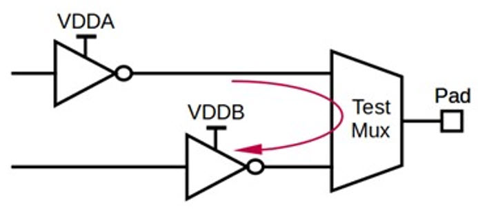
The “resulting I/O” issue can be major your first time through. Here you are with these humongous FPGAs, each with a kajillion gates. Seems like there should be plenty of rooms at the inn, right? Then you start partitioning the logic among them and you run out of pins. I/O multiplexing is a big issue, and the tools again have features to help automate this part for you, but the price you’ll pay is speed.
Tip Four: Consider the Tradeoffs
It’s important to remember that, like most engineering decisions, using a prototyping methodology has pluses and minuses.
On the plus side, your design will execute much, much faster than it would using software simulation. It’s feasible to develop and debug even complex software and interactions between software and hardware using a prototyping methodology. Also, it’s possible to stimulate your design using actual signals from real hardware instead of relying exclusively on simulation vectors.
On the minus side, with your whole design locked away deep inside a cluster of FPGAs, you don’t always have access to all the signals that you need to look at to find your bugs, as you would using a traditional simulation technique. A lot of the third party software and hardware vendors have gone to great lengths to improve this situation in their prototyping environments, to the point where you can usually get most of the information you need. Just don’t expect it to have the visibility and flexibility that you’re used to with simulation.
The second disadvantage is iteration time. Using a prototyping methodology, making a design change and seeing your results is typically a long and involved process, including resynthesizing the design, rerunning the partitioning, rerunning place and route, etc., before you’re ready to be up and going with a changed design. You’re running much faster, but you’re less maneuverable.
Tip Five: Understand the Benefits of Off-the-Shelf Boards
Generally, the notions of “complex” and “off-the-shelf” would be viewed as opposites. This is not the case, however, in the world of ASIC prototyping boards. Indeed, companies like Nallatech, HARDI Electronics, The Dini Group, and Gidel are key enablers for ASIC prototyping, eliminating the need to spend eons developing high-performance custom boards, and many specializing in specific application areas. Lars-Eric Lundgren of HARDI Electronics contributed a companion article this week that explores requirements and benefits of using off-the-shelf boards to create an ASIC prototype.
Tip Six: Consider Turnkey Solutions
Perhaps you’re not in a position to build your own ASIC prototyping environment, even with the help of off-the-shelf boards and commercial software. Turnkey emulators are no longer just the purview of the wealthy. Companies like Mentor Graphics, Cadence Design Systems, ProDesign, and EVE Engineering offer more complete solutions, even for designs of moderate complexity. Emulation systems typically come bundled with dedicated design software, a prototyping board or boards, preassembled in an enclosure with a power supply, cooling, etc. Investing in emulation could provide you with a more productive environment if you’ll be facing this challenge for multiple designs.
ASIC verification is a huge challenge, and it isn’t going to get easier. Prototyping with FPGAs offers the possibility of reducing verification time, but “pre-flight” preparation is a must.