editor's blog
Subscribe Now

Yet Another Way to Sense Magnetic Fields

Seems we have so many ways of detecting the magnetic fields around us! And now we have yet another.

Some years back we covered a small company called Crocus, a maker of MRAM technology. Their MRAM cell consisted of two magnetic layers: a “pinned” reference layer and a programmable layer. The idea was that, when the layers are aligned, the tunneling resistance through the combined layers and a thin layer of dielectric between them was different from when they were anti-aligned.

So by programming the top layer to be either aligned or anti-aligned, you could store data and read it back by measuring the tunneling current through the cell (hence the resistance).

The “pinning” comes by placing the magnetic layer just over a material that, in bulk, wasn’t magnetic, but at a nano-structural level, consisted of alternating layers of atoms magnetized in opposite directions. Because they were alternating, they neutralized each other overall, but for something sitting right atop the material, it felt only the top layer, so it seemed to be magnetized. And this stabilized the magnetic layer to align and stay there.

The free layer also had a pinning material like this that stabilized it during use, but the write circuitry was able to overcome that (with the help of some heat) to allow that layer to be flipped.

So that was how it formed a memory.

Then they figured out how to do logic with it: by making both layers programmable, they could effectively implement XOR logic. Sounded interesting, although I haven’t seen any actual product come of this idea.

Now they’ve morphed things yet one more time. In this case, they’ve removed the pinning layer from the top and they’ve taken away all the write circuitry (a huge savings). Now that top layer can simply spin away according to whichever magnetic fields it happens to be in. Its direction can still be measured by checking the tunneling current.

These three configurations are illustrated in the following conceptual, super-simplified figure.

Crocus_cell_dwg.png 

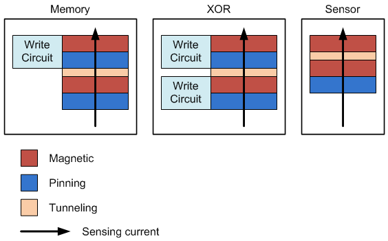
In the memory application, the current had two values – one for 1, the other for 0. In the magnetic field detector implementation, the current can take on a continuous range of values between the 1 and 0 values.

The benefits they tout include low-power sensing, linearity good enough not to need compensation, and the ability to operate as high as 250 °C.

This actually isn’t a new thing – they’ve apparently been quietly selling this stuff for a couple years, and just completed a new round of funding. But it seemed worth talking about as an example of technology being repurposed for new markets.

You can find out more on their site

Leave a Reply

featured blogs
Nov 28, 2023
Chiplet Revolution Insights from Industry Leaders The semiconductor landscape is undergoing a seismic shift as the demand for more powerful and energy-efficient electronic devices reaches new heights. In a recent panel discussion at CadenceLIVE Europe, featuring luminaries su...
Nov 27, 2023
Qualcomm Technologies' SVP, Durga Malladi, talks about the current benefits, challenges, use cases and regulations surrounding artificial intelligence and how AI will evolve in the near future....
Nov 27, 2023
See how we're harnessing generative AI throughout our suite of EDA tools with Synopsys.AI Copilot, the world's first GenAI capability for chip design.The post Meet Synopsys.ai Copilot, Industry's First GenAI Capability for Chip Design appeared first on Chip Design....
Nov 6, 2023
Suffice it to say that everyone and everything in these images was shot in-camera underwater, and that the results truly are haunting....

featured video

Dramatically Improve PPA and Productivity with Generative AI

Sponsored by Cadence Design Systems

Discover how you can quickly optimize flows for many blocks concurrently and use that knowledge for your next design. The Cadence Cerebrus Intelligent Chip Explorer is a revolutionary, AI-driven, automated approach to chip design flow optimization. Block engineers specify the design goals, and generative AI features within Cadence Cerebrus Explorer will intelligently optimize the design to meet the power, performance, and area (PPA) goals in a completely automated way.

Click here for more information

featured paper

3D-IC Design Challenges and Requirements

Sponsored by Cadence Design Systems

While there is great interest in 3D-IC technology, it is still in its early phases. Standard definitions are lacking, the supply chain ecosystem is in flux, and design, analysis, verification, and test challenges need to be resolved. Read this paper to learn about design challenges, ecosystem requirements, and needed solutions. While various types of multi-die packages have been available for many years, this paper focuses on 3D integration and packaging of multiple stacked dies.

Click to read more

featured chalk talk

The Future of Intelligent Devices is Here
Sponsored by Alif Semiconductor
In this episode of Chalk Talk, Amelia Dalton and Henrik Flodell from Alif Semiconductor explore the what, where, and how of Alif’s Ensemble 32-bit microcontrollers and fusion processors. They examine the autonomous intelligent power management, high on-chip integration and isolated security subsystem aspects of these 32-bit microcontrollers and fusion processors, the role that scalability plays in this processor family, and how you can utilize them for your next embedded design.
Aug 9, 2023
13,581 views