

In a sleepy little town of 4 or 5 houses, you can be pretty informal about how mail arrives at its destinations. People can come pick it up at the post office, or the postmaster can drop it off on the way home, or whatever works. But once you get too many houses, you have to get organized: create routes and schedules and hire delivery folks to handle deliveries in a more structured manner.
That’s what’s happened with SoCs: the ad-hoc interconnect schemes of yore are giving way to networks-on-chip (NoCs) so that the complex communication interplay between blocks can be carefully designed, managed, and tuned.
Which is good, except that a NoC is a complex animal, and, traditionally, it goes into the chip layout mix as part of the whole – it’s just another (complex) bit of IP. Layout affects performance, so tuning and closing the timing of a NoC in the middle of the rest of the layout would presumably be a difficult proposition. It also adds a significant burden to the EDA tools trying to manage the whole thing.
So Arteris has a proposal: segregate the NoC that from the rest of the circuit and optimize it independently. This relies on a layout that provides channels between IP instances where the NoC lines and circuits will be placed.
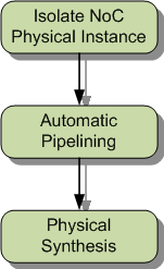
They describe a three-step process starting after initial layout. First, the NoC IP is isolated so that timing and routing can be optimized. In the second part, pipeline stages are automatically added (as they point out, you’ll never get from point A to point B across a 28-nm chip in one clock cycle). Finally, timing is closed using physical synthesis – which they claim can provide single-pass success.
This lets you optimize the NoC unburdened by the rest of the SoC, and it lets the EDA tools handle the rest of the SoC unburdened by the NoC. Arteris says that this divide-and-conquer approach gets you to tape-out faster than trying to do the whole thing at once.
You can read more in their announcement.


