

Seems like no aspect of IC design and production escapes the need for All Things to Get Harder and Harder, requiring ever-better solutions. Today we look at reticle inspection, and, in particular, at KLA-Tencor efforts to adapt their Teron system, originally intended for mask shop use, to the needs of production fabs. The idea is that, when new reticles come into the fab, they need to be inspected as a basic QC step. And, after 300-600 or so uses, they need to be re-qualified to make sure that acquired defects aren’t reducing die yield.
One practical consideration is floorspace. The volume of reticles is increasing due, for example, to multiple patterning, which multiplies the number of reticles for some layers. 14-nm flows literally double the number of reticles as compared to 20 nm. No one wants to add more machines to handle the extra load; fab managers would rather increase the processing capabilities of the “space” currently allocated to inspection, placing an extra burden on the equipment.
So what kinds of defects are the inspection systems looking for? There are several, but haze seems to be a big one. Haze represents the slow deposition of chemicals – presumably from various other processing steps – onto the reticle. Obviously the best solution is to eliminate the sources of the haze, and progress has been made on that, but some remains – and, of course, it’s now harder to detect.
For one thing, it used to predominate in open spaces, where it’s easier to pick out. Now it tends to collect along the sides of features, making it harder to see. Also, because there’s less haze, you’re looking for smaller, more isolated defects than before, when a cloud-like collection would be more evident. The presence of optical proximity correction (OPC) features makes this harder, since they can be hard to distinguish from defects.
Other things to look for include evidence of the chrome, which makes up the actual pattern, “migrating” – narrowing or flattening after cleaning, as well as simple “fall-on” defects that won’t fall off.
So how do you go about finding these things? There are a number of techniques, some of which work and some of which no longer do. In the end, a combination works best.
- Simple optical inspection can be used, but it has to be “actinic” – that is, use the same wavelength of light that will be used during wafer patterning: 193 nm.
- For repeating patterns, it used to be helpful to compare neighboring versions of the same feature. But that is less useful today because, even though the original layout of each cell may be the same, the OPC features may be different, so the cells are no longer identical on the reticle.
- Production reticles often have more than one die instance, so it can be useful to compare neighboring dice on the reticle. But for leading-edge processes, single-die reticles are more common – as are shuttle wafer reticles, which have multiple dissimilar dice that can’t be compared. So this technique isn’t so useful anymore.
- Modeling can help. KLA-Tencor generates models offline and uses them in real time to compare to what’s actually being seen.
- KLA-Tencor also uses a technique that they consider to be one of their differentiating strengths: a “difference image.” They capture images of how light is transmitted and reflected through the reticle. From each of those, they calculate what the other ought to look like. So, for instance, from the reflected image, they calculate what the transmitted image would be in the absence of any defects. And vice versa. They can then subtract the calculated versions from the observed versions – calculated transmitted vs. observed transmitted, and likewise for reflected – and use the differences to pinpoint defects. This is a compute-intensive operation that places a heavy load on the inspection equipment.
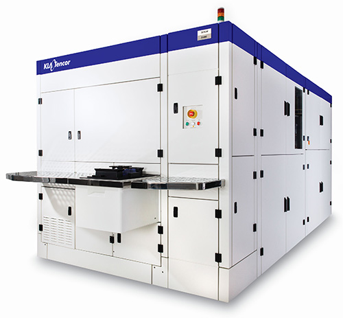
The processing power they’ve built into their just-announced Teron SL650 is intended to handle the inspection complexity with a high signal-to-noise ratio while still accommodating the increased number of reticles it needs to handle.
(Image courtesy KLA-Tencor)
You can find more on the new system in their announcement.


