editor's blog
Subscribe Now

Tree Frogs Help Graphene Grow

Growing high-quality graphene for use on wafers is hard. Chemical vapor deposition (CVD) is the favored approach, but no one has perfected the ability to grow it directly onto the oxide surface of a wafer.

It’s much easier to grow it on a sheet of copper and then transfer it over. But that transfer step can be tricky, and copper isn’t a perfectly uniform, crystalline material either. So defects can easily result.

One obvious trick might be to put copper on the oxide, grow the graphene on that, and then etch the copper away, leaving the graphene on the oxide surface. This technically can work, but the graphene tends to lift off the surface before it can be secured in place.

So… it would be useful to find a way to hold that graphene layer before it’s baked down. And if you were looking for a way to get something to adhere to a surface, where would you look in nature for ideas?

Why, tree frogs, of course!

Tree_frog_red.jpg


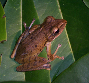
Image courtesy W.A. Djatmiko (Wikipedia)


It turns out that tree frogs stay attached to underwater leaves thanks to nano-sized bubbles and capillary bridges between leaf and foot. Some beetles do a similar trick.


Well, this idea has now been transferred to graphene. Prior to laying down the copper, the wafer surface is treated with nitrogen plasma. Copper is then sputtered on and CVD deposits the carbon. The carbon is then etched, and, during that process, nano-bubbles form, creating capillary bridges. These hold the graphene in place as the copper disappears.


A final bake step secures the graphene to the wafer and eliminates the bubbles and capillaries.


You can read more about this in their paper, but it’s behind a paywall.

Leave a Reply

featured blogs
Mar 31, 2023
Learn how (and why) the semiconductor industry is moving towards chiplet-enabled multi-die systems in our research piece in MIT's Technology Review Insights. The post An Industry-Wide Look at the Move Toward Multi-Die Systems appeared first on New Horizons for Chip Design....
Mar 31, 2023
The Verisium Debug platform is optimized for scalability, supporting debugging of simulation runs and emulation, where support for loading large source files and handling huge amounts of probe data is a must. Join this free Cadence Training Webinar to learn how to automate yo...
Mar 30, 2023
Are you in desperate need of a program manager to instigate a new project or rescue an existing project that is spiraling out of control?...

featured video

First CXL 2.0 IP Interoperability Demo with Compliance Tests

Sponsored by Synopsys

In this video, Sr. R&D Engineer Rehan Iqbal, will guide you through Synopsys CXL IP passing compliance tests and demonstrating our seamless interoperability with Teladyne LeCroy Z516 Exerciser. This first-of-its-kind interoperability demo is a testament to Synopsys' commitment to delivering reliable IP solutions.

Learn more about Synopsys CXL here

featured chalk talk

Beyond the SOT23: The Future of Smaller Packages
Sponsored by Mouser Electronics and Nexperia
There is a megatrend throughout electronic engineering that is pushing us toward smaller and smaller components and printed circuit boards. In this episode of Chalk Talk, Tom Wolf from Nexperia and Amelia Dalton explore the benefits of a smaller package size for the SOT23. They investigate how new package sizes for this SMD can lower your BOM, decrease your board space and more.
Oct 20, 2022
21,498 views