

It’s ITC time, and this is when many of the EDA and test folks roll out their new stuff. True to this pattern, Synopsys has announced two new offerings, one of which allows faster SoC testing, the other allowing faster design of the test infrastructure in an SoC.
The first is a rather significant upgrade to their design-for-test (DFT) offering. Called DFTMAX Ultra, it’s a from-the-ground-up revamp of their test compression technology. It addresses compression, test speed, and the number of test pins.
They’ve completely redone their compressions scheme, resulting in 2-3X better compression. This includes improvements in fault models (since more subtle types of faults need to be caught now) as well as better handling of X (don’t know/care) values, allowing better propagation of fault values to outputs without being masked by some X.
They’ve also pipelined their engines so that they can be clocked faster: up to 60 MHz. And instead of the old model, where you load up a pattern, test it, and then unload it, you can now run tests in a streaming mode. So you don’t wait until everything is loaded to test, and you don’t wait until everything is unloaded to start the next test. Better – and less – use of test time.
They also allow better control over how many test pins you want to use. This is becoming more of an issue for test beds that do “multi-site” testing. If a given number of pins is now going to drive two chips instead of one, then each chip has to be able to live with half of those pins instead of all of them. So you can dial the number of pins down all the way to two. The compression goes up, of course, when pins come down, so there is a tradeoff, but the tool gives you that capability.
Combining these improvements together gives a test performance improvement of 20X (even up to 30X for some designs).
Separately, they’ve announced a product addressing the integration of IP tests into a full-on SoC test scheme; they call it the STAR Hierarchical System. The issue is that you buy a piece of IP that comes with test vectors and such so that you can validate it. But that IP will eventually be buried inside your SoC without direct IP I/O access to the tester (most likely). So you have to be able to fold all of the IP together into a single SoC set of tests.
The STAR hierarchical system helps perform this integration by setting up an infrastructure of “servers” and wrappers for managing the individual IP tests.
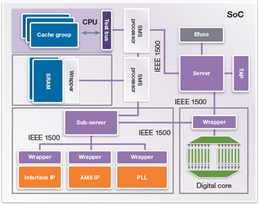
You can access IP blocks for testing and debug either on an IP block level, a subsystem level, or at the level of the SoC. The system is P1687 compatible for efficient debug, and it supports e-fuse programming for calibration.
Since the tests for each IP block are independent of the tests for other IP blocks, you can save test time by running different IP block tests in parallel. Their system helps you schedule which runs alongside which to optimize the test runs.
So while DFTMAX Ultra is focused on making an actual test run faster, the STAR Hierarchical System is focused on making it easier to create the test infrastructure and test vectors during design time.
You can find out more about both products in their announcements: DFTMAX Ultra here and STAR Hierarchical System here.


