

mCube made more noise recently with their announcement of a very small, low-power accelerometer. There were a number of aspects to the release; some intriguing, some… less so.
Let’s start with intrigue. The whole focus here is on a small device that can be used in space-constrained, power-stingy applications – like wearables. Obviously space is critical in any such device, but they point out that flexible circuit boards can enable more… well… flexible shape designs. And, while the accelerometer isn’t itself flexible, the closer you can come to an infinitesimal point on a flexible board, the more likely your connections are to remain intact. So, on flex boards, small=reliable.
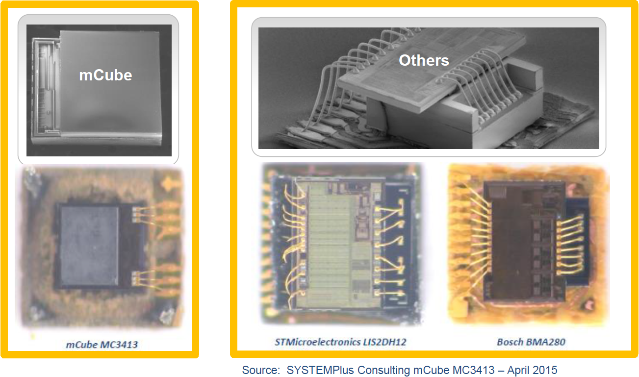
They get the size by stacking a MEMS wafer with through-silicon vias (TSVs) over a CMOS wafer (all of which is then garnished with a cap wafer). This means that bond pads are needed only for actual connections to the outside world, not for intra-package die-to-die connections, which can take a lot of space.
Cost is also mitigated by using an old process with fully depreciated equipment. Right now, they’re at 180 nm; they could go to 150 without spiking the cost curve. In addition, all of the steps – from the different wafers to bonding them – are done in a single fab. This is as compared to other processes, where wafers have to be bundled up and sent to different fabs for different parts of the process.
They’ve also built in a couple key application-oriented features intended to go easy on battery life. First, you can tune the sample rate – fast for tablets and phones that need to be responsive enough for games (a couple thousand samples per second), slower (400 samp/s) for wearables. Second, they have power modes: a normal mode at 4.7 µA (50 Hz), a single-sample mode at 0.9 µA (25 Hz), and a “sniff mode” at 0.6 µA (6 Hz).
Sniff mode monitors for activity, sending an interrupt when detected. The threshold for what constitutes “active” can be tuned to suit the application.
So, functionally, this seems to compete pretty well. Which is really all that should matter. The less intriguing bits have to do with the marketing and what feels like playing a little loose with terminology. Any good marketer knows that it’s great if you can carve out for yourself a new market or “category” so that you have no competition. Problem is, too many folks have read that in their business books, and try it too often.
Here, mCube is trying to define the “IoMT” – Internet of Moving Things – as a separate thing. This suggests that, somehow, items with IMUs constitute this separate class of system. Sorry, but it just doesn’t work for me.
A little more worrisome is their use of the word “monolithic.” As in, they’re claiming a monolithic solution. First, “monolithic” literally means “from one stone.” This is not from one stone – it’s from three wafers. Monolithic would be if the MEMS and CMOS were fabricated out of the same wafer. (I won’t quibble about the cap wafer.)
They even use this to distinguish themselves from InvenSense, who uses what they call a “stacked” approach. They say that this distinction is significant enough to define the end of “Sensors 2.0” and the beginning of “Sensors 3.0.” Again, more new categories. Again, not working for me.
The only real difference here from InvenSense is that InvenSense inverts the MEMS wafer and bonds face-to-face (and does this in some other fab, by implication). mCube stacks bottom-to-top, connecting with TSVs. That has some benefits – don’t get me wrong – but it doesn’t feel to me like the revolutionary birth of a new category.
OK, kvetching over. You can find more information about the tiny new mCube accelerometer in their announcement.


