

AI in edge devices is expected to experience mind-blowing growth over the next half decade, with predictions exceeding 100% CAGR. That means our IoT devices are going to be getting smart, and doing it quickly. Most of the applications of AI in edge or endpoint devices centers on sensors. Our devices are equipped with increasing numbers of increasingly complicated sensors, drowning our devices in data. In most applications, however, it isn’t practical to simply push all that raw sensor data up to the cloud for further processing. We need to make some sense of it now, at the edge, embedded inside our device.
Most AI schemes involve discrete steps for training and inferencing. Training can be accomplished at our leisure in computing-rich, floating-point-having, plentifully powered heavy iron computing environments. Then, for in-the-field inferencing, the trained machine can be ported to our embedded system in a way that allows hyper-efficient, real-time analysis at the edge.
This week, at the 2018 Embedded Vision Summit in Santa Clara, Lattice Semiconductor will unveil sensAI, the most recent FPGA-based platform and ecosystem aimed at enabling AI at the edge for a variety of applications including mobile, smart home, smart city, smart factory, and smart car. Lattice says sensAI is a “complete technology stack” that combines modular hardware kits, neural network IP cores, software tools, reference designs, and custom design services – all aimed at accelerating the development of machine learning inferencing for IoT edge devices.
Lattice says sensAI is “Optimized to provide the ultra-low power (under 1 mW–1 W), small size, and production-priced (~$1-$10 USD) benefits of ASICs, with FPGA flexibility to support evolving algorithms, interfaces, and tailored performance.” Interestingly, Lattice has built their solution around two different FPGA options. The ECP5, which is the fifth generation of Lattice’s value-based FPGA, handles the “high end” of the sensAI solution, where video processing is required, and applications that require less performance, smaller form factor, and ultra-low-power consumption can use iCE40 UltraPlus – a tiny FPGA based on technology gained with the acquisition of SiliconBlue several years ago.
It’s safe to assume that the Lattice engineers who created the initial ECP FPGA family (internally dubbed “el-cheapo” at the time) and the SiliconBlue engineers who created the predecessor to today’s iCE families would never have guessed that their designs would someday be powering neural networks to extract features from sensor data in IoT edge applications. In both cases, the FPGA architecture was originally designed to fill a niche where more expensive and power-hungry FPGAs from the large suppliers couldn’t work. These were glue-logic devices whose role in life was to fill the lucrative but unglamorous role of bridging interfaces and handling the messy interstices of larger logic designs. Now, the descendants of those chips have found new and exciting life in leading roles on the front edge of today’s technology curve.
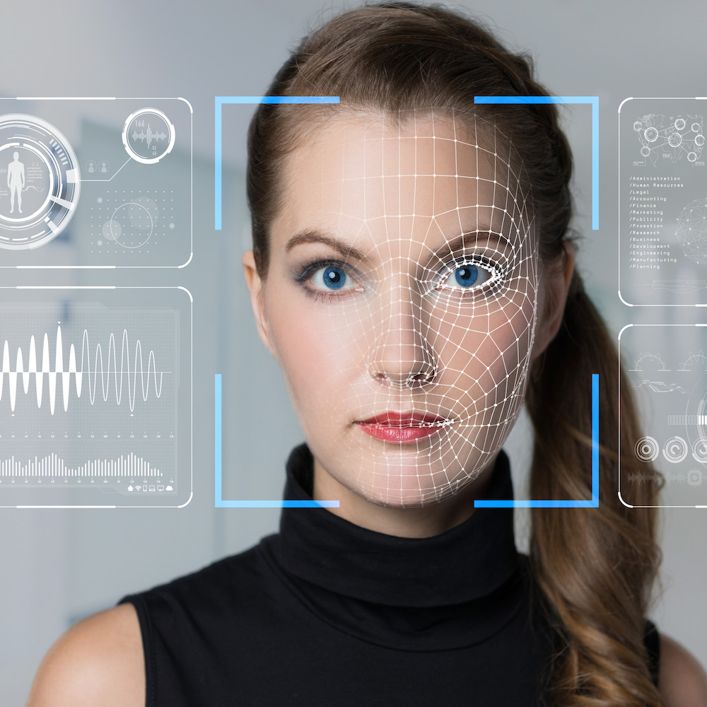
Lattice’s solutions include two modular hardware platforms – the ECP5™ device-based Video Interface Platform (VIP), which includes Lattice’s Embedded Vision Development Kit, and the iCE40 UltraPlus device-based Mobile Development Platform (MDP) aimed at handheld and battery-powered devices. Both solutions bring AI-specific IP cores such as a Convolutional Neural Network (CNN) accelerator and a Binarized Neural Network (BNN) accelerator. They also include a neural network compiler tool for Caffe/TensorFlow to FPGA, in addition to the usual Lattice “Radiant” and “Diamond” FPGA development packages. To get you jump-started on your AI implementation, Lattice includes reference designs such as face detection, key phrase detection, object counting, face tracking, and speed sign detection. These are some of the most common types of applications for design teams wanting inferencing at the edge, and they also provide good exemplars for similar applications.
Lattice says that their solutions are “optimized for ultra-low power consumption (under 1 mW–1 W), small package size (5.5 mm2 –100 mm2), interface flexibility (MIPI® CSI-2, LVDS, GigE, etc.), and high-volume pricing (~$1-$10 USD). In each case, you can assume that the lower end of those numbers is the iCE-based solution and the higher end the ECP5. Putting the stack to work at two distinct points on the power/performance/cost curve is a slick move by Lattice, taking their silicon and solutions to a broader set of applications and positioning themselves as an edge-AI supplier with more than one trick up their sleeve.
Because AI can be intimidating for many engineering teams, Lattice has partnered with a number of design service companies to deliver custom solutions for broad market applications, including smart home, smart city, and smart factory. If you don’t want to dive into the deep end of AI world on your first try, it’s nice to know that there is expert help available for most of the common types of applications, and that those experts are already competent with Lattice’s solution and ecosystem.
Last week, we looked at a similar edge-based AI solution, QuickLogic’s QuickAI ecosystem, and, while the two offerings have similar goals, it is interesting to see the two differing approaches side by side. In the case of Lattice, the solution relies more heavily on the FPGA component, implementing the neural network inferencing as FPGA IP. In QuickLogic’s case, the neural network load is handled by stand-alone neuromorphic processors. This may make Lattice’s solution a bit more “one stop shopping” and possibly more BOM-friendly (looking at the entire solution), while QuickLogic’s ecosystem may bring more neural network performance and scalability because of the specialized neuromorphic chips included in their offering.
AI at the edge tends to be mass market by its very nature. The compute challenge is posed by large numbers of sensor-laden nodes processing piles of data at the edge when uploading to the cloud is impractical. That means the platforms addressing the issue have to be mass market friendly, with BOM costs at a minimum, power consumption under control, and backed away from the bleeding edge on form factors that would make board cost prohibitive. Since Lattice has spent the last decade focusing on consumer and mass-market applications, the company is well acquainted with the requirements for delivering solutions in that market, and that experience should serve them well as they attack the AI opportunity.
It is interesting to see the evolution of Lattice from a “me too” FPGA supplier to a leader in their own right in rapid-growth markets that traditional FPGA companies have passed by. As the technology landscape shifts with the slowdown of Moore’s Law, the explosion of AI, and the rapid deployment of IoT technology, it’s anybody’s guess as tp which pieces of technology will become the must-have defensible solutions that capture emerging key markets. AI at the edge seems like a pretty good bet.


One thought on “More AI at the Edge”