

Well, it looks like we just might have ourselves something of a tussle playing out deep in the corner of your friendly neighborhood silicon fab. Applied Materials has announced a new way of approaching atomic layer deposition (ALD), but others say, “Not so fast…”
Before we can tackle the nuances of what’s going on here, let’s back out and review what ALD is all about. We keep hearing about how dimensions in ICs are shrinking to atomic levels – which, in some cases, is a certain level of hyperbole to drive home just how much of a challenge silicon processing has become. But, in a few cases – and in more cases to come – we really are talking about films that are literally a few atomic layers thick. High-? gates, metal replacement gates, and DRAM trench capacitors and electrodes are all examples that currently require ALD. New 3D structures will need more.
So how the heck do you deposit a layer that’s only one or a few atomic layers thick? Certainly not by sputtering or anything quite so crude – by comparison, that’s like putting a film of peanut butter on your bread with your elbow. No, there’s a really clever way it’s done in a two-step process.
You start with one precursor gas. It’s a compound that includes some component of the molecules you want in the final film. You fill the chamber with this gas, and it sticks to whatever substrate is down there. Obviously you can’t just count on this – a well-selected precursor must want to stick to what you want it to stick to.
But the thing is, it wants to stick to the substrate more than it wants to stick to itself. In other words, once the substrate has been covered and there’s no more exposed, you’re done. (I hope I’m not overwhelming you with the intricate chemistry jargon and obscure math here…)
First off, this is one of the valuable things about ALD: because the reagents go in as a gas, they permeate space in all directions and cavities (given sufficient time and large enough openings – and they don’t have to be particularly large). This means that you get an extremely conformal coating – it will follow all the ups and downs and upside downs of the substrate surface. No issues of ion directionality or step coverage or whatever. This is becoming a big deal with newer 3D structures.
So we have this monolayer of precursor 1. Next comes – wait for it – precursor gas 2. Bet you didn’t see that coming… This precursor likes to stick to the first precursor layer. And, as with the first one, it doesn’t like to stick to itself particularly much. So when the first precursor monolayer is completely covered, the second precursor’s work is done.
Then comes a “treatment” of some sort – higher temp, plasma, a cure – it depends on the chemistry. But the idea is that the two precursor monolayers react to form a single layer of whatever it was you wanted to create. And the key is that you get exactly one atomic layer.
What if you want, say, 5 atomic layers? Then you rinse and repeat four more times.
Yes, I’ve been pretty vague on the chemistries here – it depends on what you’re laying down. (And I’m not a chemist… but that was probably obvious by now.) Some typical finished films are nitrides and oxides of titanium and silicon as well as aluminum oxide.
To understand the disagreement better, we need to go another step deeper into how ALD is traditionally performed. Today’s ALD reaction occurs all in a single chamber. A wafer is placed in the chamber, and then the chamber is filled with precursor gas 1. After sufficient time, the chamber is purged to get rid of any last traces of that first precursor gas. Then the chamber is filled with precursor gas 2 – possibly followed by a thermal or plasma treatment of some kind.
The chamber can then be purged once more, and this cycle can be repeated as many times as necessary to get the desired thickness.
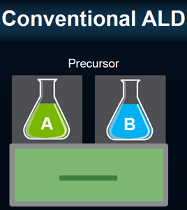
(Image courtesy Applied Materials)
Applied’s point is that this whole purging thing uses precious time. And it can result in high maintenance: the chamber walls are also subjected to this deposition, and they occasionally need to be cleaned. What if, instead of having a wafer sit in one place with the gasses being swapped, you had two different zones, each with one of the gasses, and you move the wafer from one zone to the next? No purging would be needed, and neither chamber wall would see both precursors (in other words, you wouldn’t get as much build-up).
If you’re like me, you would expect that there would be an airlock between the zones to keep the precursors from comingling. But – and here’s the mysterious part and the source of some debate – Applied has no such airlocks – they claim not to need them. They merely have a “chemistry-free” zone between the two precursor zones. And they’re not saying how they’re doing that.
We could view this process as a linear one: wafer moves from gas 1 to gas 2 to the selected treatment and acquires a shiny new layer of some atom. It’s an easy way to understand the fundamental concept. But if you want to cycle for more layers, well, you want a circle. So they’ve got this rotating platform, and the wafer basks in the gas 1 zone and then rotates around to the gas 2 zone – and then back to gas 1 for the next layer.
A treatment can be done in between, but they’ve modularized this so that the treatment is decoupled from the gases, providing more flexibility.
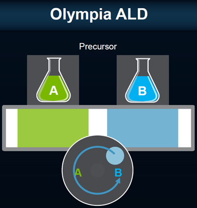
(Image courtesy Applied Materials)
Sounds pretty slick. But at Semicon West, I also happened to talk to ASM, who describe themselves as currently the number 1 ALD equipment supplier. And they’re sticking with the traditional approach. They say that they’ve seen the zone concept before and aren’t completely bought off.
You might say that this is a natural response from a company that needs to defend its turf, but they gave some specific reasons. In fact, they claim to get better control with their approach. The purge can be “cleaner” than the rotating platform. They say that small amounts of gases can move from one zone to the other (my guess, for instance, would be in a boundary layer near the surface… but it’s just a guess).
As to the wasted time purging, they concede that for simple, planar depositions, the Applied approach might be faster. But for complex 3D topologies, the dominant delay is the amount of time you have to wait to allow the gasses to make their way into all the nooks and crannies – that makes the purge time less of an issue.
They are also making their chambers smaller. That makes for lower gas capacity, meaning less gas to purge, making the purge faster.
Are these claims solid, or are they marketing bluster in defense of incumbent equipment? Hard for me to say. (They certainly seemed sincere when discussing it…) I haven’t seen any numbers attempting to prove one or the other approach as better. And, of course, there’s Applied’s big mystery zone-separation technology, whose effectiveness I have to take on faith.
So it remains a topic that diligent buyers will need to address when deciding which machine will get that coveted floorspace. With all the ALD anticipated in the coming years, there will be plenty of such purchases to prove this out.
More info:
Applied Materials Olympia ALD System


What’s your take on the best approach to atomic-layer deposition?