


I’ve always found ISSCC to be a useful exercise. If nothing else, it puts me in my place if I ever start thinking I know a lot. ISSCC reminds you how little you know compared to the hordes surrounding you. It’s an exercise involving me desperately trying to keep the tip of my nose above water while the presenters all around me make waves.
The available topics vary widely, with some remaining consistent over the years and others coming and going. Energy Harvesting now has its own session, and I spent some time there experimenting with how well I could track the presentations.
So this is for those of you following the low-level things that are gradually making harvesters more efficient and useful. We’ll cover three specific threads: DC-DC converters, multi-source harvesters, and maximum-power-point tracking (MPPT). I’ll run through a summary of all three here; I’ll refer you to the specific session for all of the glorious details (for those of you with access to the proceedings and suitable synapses).
Converting more power
When it comes to power conversion, DC-DC converters used for energy-harvesting have far more of a challenge than do the converters in more traditional settings. The whole thing about energy harvesters is to be able to deliver sufficient power to a load. As odd as it may seem to have to think about this, the problem is that the circuits used to convert the power can’t consume all – or much – of the power in the process. If you send someone out for ice cream, it’s no good if they eat all the ice cream on the way back. You want the maximum net ice cream, which preferably means sending someone that doesn’t even like ice cream.
Such a choice isn’t really available in circuits – they all consume something, but three of the four papers dedicated to conversion derived their challenges from minimizing power loss. The first paper in particular addressed an approach that provided a good voltage boost but poor power conversion efficiency (PCE). How could that be? Because it wastes current somewhere along the way. Bear in mind that, in most of these cases, voltages are small, so leakage can be a dominant player.
That first project, a partnership between Hong Kong University and Seoul University, focused largely on the body biasing used to improve conductance of the switches (which are just FETs). Prior schemes used forward body biasing (FBB) on the NMOS transistors, but this could result in rush currents – clearly killing the PCE.
So this project used switched body biasing (SBB), with the NMOS transistors in deep wells. By moving the body voltage around, they could keep any parasitic diodes from turning on. But it turns out it’s not quite so simple. In order to guarantee that no short-circuit currents occur, some of the internal switching signals must be non-overlapping, with a dead time between to accommodate the relatively slow clock transitions. Question is – how long to make that dead time?
That turns out not to have a simple answer. If the length is too short, then you run the risk of short-circuit currents; if too long, then you don’t capture as much of the power as you could because you’re waiting around. It also depends on the input voltage: the dead time tends to move out with lower voltage.
So the team took an adaptive approach, creating both short and long delays and then muxing them: long when the input voltage is high, short when it’s low.
The second project, involving MIT, UCSD, and a couple of Boston medical institutions, was for an endocochlear implant – a widget that fits deep in the ear. This is the home of the “endocochlear potential”, or EP: 70 – 100 mV that’s involved in the hearing process, but which can be tapped for generating up to 6.26 nW (limited by physiological constraints). This is an exceedingly low power level, so every last drop of anything counts. The work done here was all about optimizing impedances and clock timing.
The results of that work took the quiescent power down into pW territory: 544 pW, to be precise.
An interesting note with this paper was that of start-up. This gets to one of the questions people tend to ask a lot, since many of these circuits look fine once running, but they have to bootstrap themselves. I recall last year seeing a circuit that went through about four stages of power up, each stage enabled by the power of the prior stage. In the case of this endocochlear implant, it can’t bootstrap itself: an antenna allows the circuit to be started using a burst of RF energy delivered by the doctor outside the ear itself.
The third project came out of the University of Michigan. They noted that, if circuit size is an issue, switched-capacitor converters are preferred to ones involving inductors. But the clock generation and level-shifting circuits required use too much power in these micro-power applications. So their approach was to use oscillators that started themselves up and generated the clock signals.
These oscillators are, in principle, simply replications of the switched-cap network (SCN) that was already in the voltage doubler. They took out the clock generator and level shifters and replaced them with some number of extra SCNs. Each stage has a top oscillator, which switches between a medium and a high voltage, and a bottom oscillator, which switches between that medium voltage and a low voltage. They’re connected by the flying capacitors and synch up in frequency and amplitude.
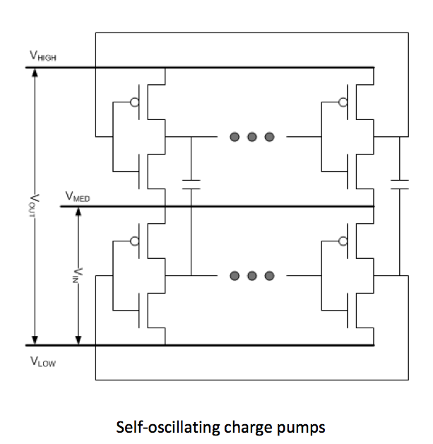
Output power is 5 nW to 5 µW; quiescent power is under 3 nW.
The last of the converters deals with voltage limits in a paper done by UCLA and SiTime. The issue for them is the growing use of MEMS oscillators. The problem is that they can run more efficiently biased at higher voltages, but the increasingly aggressive silicon nodes limit how high you can go without causing breakdown. So they did a hybrid design that combined different charge pumps having different tolerances and efficiencies.
They used three different types of charge pump (each of which had multiple stages). The first used standard CMOS doublers, with all wells tied to their standard levels (efficiency of 88%; voltage limit of 12 V). The second stage was similar, except that it was all NMOS, with the n-wells biased to the output of the first stage – 12 V. The effects of diodes and back biasing reduced the efficiency to 42% but got the voltage up to 20 V (the 12-V starting plus an 8-V breakdown limit). The final stage was very different, using so-called Dickson charge pumps, which involve polysilicon PIN diodes built over shallow-trench isolation. That stage had efficiency of only 29%, but it took the voltage capability up to 88 V.
They used metal-fingered capacitors, sized to ensure reliability, to be sure that the caps could handle the higher voltages. The overall circuit can generate up to 34 V from a 2.75-V input and can sustain over 30 V output for loads under 10 µA.
Multiple sources
The next couple of papers dealt with multi-source issues. Although they did so from different angles.
In the first, from Georgia Tech, the two “sources” are storage: a fuel cell and a lithium-ion battery. Why two energy sources like this? Because the fuel cell stores more energy – 5-10x that of a lithium ion battery of similar weight; it just can’t always release it as quickly as might be needed. For that, the lithium ion battery can step in, providing power 10-20x that of the fuel cell.
A use case for this is suggested by wireless sensor nodes. Mostly they sleep. Occasionally they sense – requiring nominal power. After sensing, or after some number of sensing events, they establish a wireless communication connection with the mother country in order to repatriate the data or receive instructions. That radio thing takes a lot of power, and that’s where the Li battery can help.
They generalized the discussion to two sources, one “energy dense,” the other “power dense.” So they’re clearly looking beyond the specific chemistries we’ve started with.
Because the energy-dense source runs most efficiently under constant load, it’s used for the majority of the duty, with the power-dense source stepping in as needed. Any excess energy-dense energy (due to light loading) can be used to recharge the power-dense source.
Of course, they needed to design the controls that switch between the various modes. The high/low-load switching, in particular, is done hysteretically (to avoid it operating hysterically). And their big goal was to do this with a single inductor in order to save space. Beyond that, I’m not even going to try to explain how they made this happen, since it hurts my brain too much there’s not enough space.
The other multi-source paper, from KAIST (Korea Advanced Institute of Science and Technology) dealt with multiple harvesting sources: a thermoelectric generator (TEG) and a piezoelectric generator (PZT). That said, it seems that most of the focus of the paper is on the PZT; the TEG mostly goes along for the ride. In fact, it wasn’t really clear why these two were cohabitating, but it certainly posed a greater challenge to do their PZT shenanigans while the TEG was steadily working away.
The big challenge they had was in using PZT resonance. They noted that, in the past, resonance was exploited far below its potential because the voltages were limited to some value below what the oxide could handle – like double the original PZT swing. As the presenter phrased it, they were “leaving money on the table.”
So their goal was to let the resonance build until it was clamped at the limits of what the CMOS process could endure without breaking down. They refer to this as “piling up,” which is a pretty descriptive term. In general, they switch back and forth between an “energy pile-up mode” and an “energy transfer mode,” during which you send energy to the load.
I’m again going to bail on the details, except to award them Best-Named Block for their “Resonance Interceptor” block (best articulated in your most awesome basso profundo). Damn, that sounds badass. It totally makes their “Peak Value Checker” block sound like the poor sap that tells you how much you saved when handing you your receipt at the grocery store.
Tracking the max
Finally, we look at two papers on maximum power point tracking (MPPT), which lets harvesters operate at maximum efficiency in the event of changing conditions that move the optimal operating point. Both of them deal with limitations in the way tracking is done to date.
The first paper, from the University of Texas in Dallas, deals with solar cells under partially shaded conditions, which can change often and quickly as birds fly by and branches blow in the wind. If not extracted at the optimal point, they say that as much as 30% of the available power can be lost. Of particular note is the fact that individual cells will have different sunlight intensity, since (by definition of “partially shaded”) not all will be shaded equally. So one MPP won’t work for all cells.
The other MPPT project, from Korea University, involved a PZT harvester. The variations here, rather than being shading, deal with frequency and other conditions affecting the optimal operation of the vibrating piezoelectric material.
The typical MPPT algorithms have been search-oriented, either “perturb-and-observe” or “hill-climbing.” And they tend to get stuck on local maxima rather than finding the global maximum. While both projects dealt with many details surrounding the efficient conversion of power, their main claim to fame is being able to track the maximum power point much more quickly.
The Dallas project claims to be able to “instantaneously” find the global maximum, cycling back and forth between a mode where the MPP is established and then a steady-state mode (the timing of which can be programmed). The Korea project can establish the MPP in a single PZT vibration cycle, as compared to 10s or 100s of cycles for current approaches.
And I think it’s now time for me to dunk my head in some cold water (or cold beer), since it has by now been taken far from its optimal performance point.
More info:
Al of these papers are from Session 23, 2014 ISSCC.


What do you think of these ideas aimed at improving the performance of energy harvesters?