

QuickLogic has been focusing hard on sensor fusion for a while, and we have looked at their ArcticLink solution in the past. The first versions consisted of a combination of hard logic, dedicated microcode processor, and FPGA fabric. And the focus was on low power.
Apparently this has done well enough to make them double down on the investment. But their new SoC is different enough that they gave it a new name. While the old devices were called ArcticLink, they’ve now dubbed their new device EOS (after the goddess of the dawn).
It targets both phones and wearables, and it’s predicated on the fact that new algorithms (voice trigger, indoor navigation, motion-compensated heart rate, etc.) require in the range of 10-20 MIPS each (additive as you add more functions), and that 10 mW is the magic cutoff that OEMs don’t want to exceed. So the question is, how many such functions can be implemented and still stay within the power budget?
Let’s start at a high level. The old devices were simply slaves in a larger system; you needed a host in the system. EOS, by contrast, can live on its own – a feature they tout for wearables, where the number of components and the power they consume are particularly delicate.
So EOS consists of the stuff that ArcticLink has – indicated in various shades of green below – plus a number of other blocks that allow the device to be autonomous. Functionally, whether or not it accompanies another device, this is intended to act as the “always-on” manager for the system, since they claim it will consume less power than any microcontroller-based sensor hub. So even if this sits in a phone next to an application processor with an integrated sensor hub, EOS is intended to handle the always-on sensing since it will consume less energy than that integrated hub.
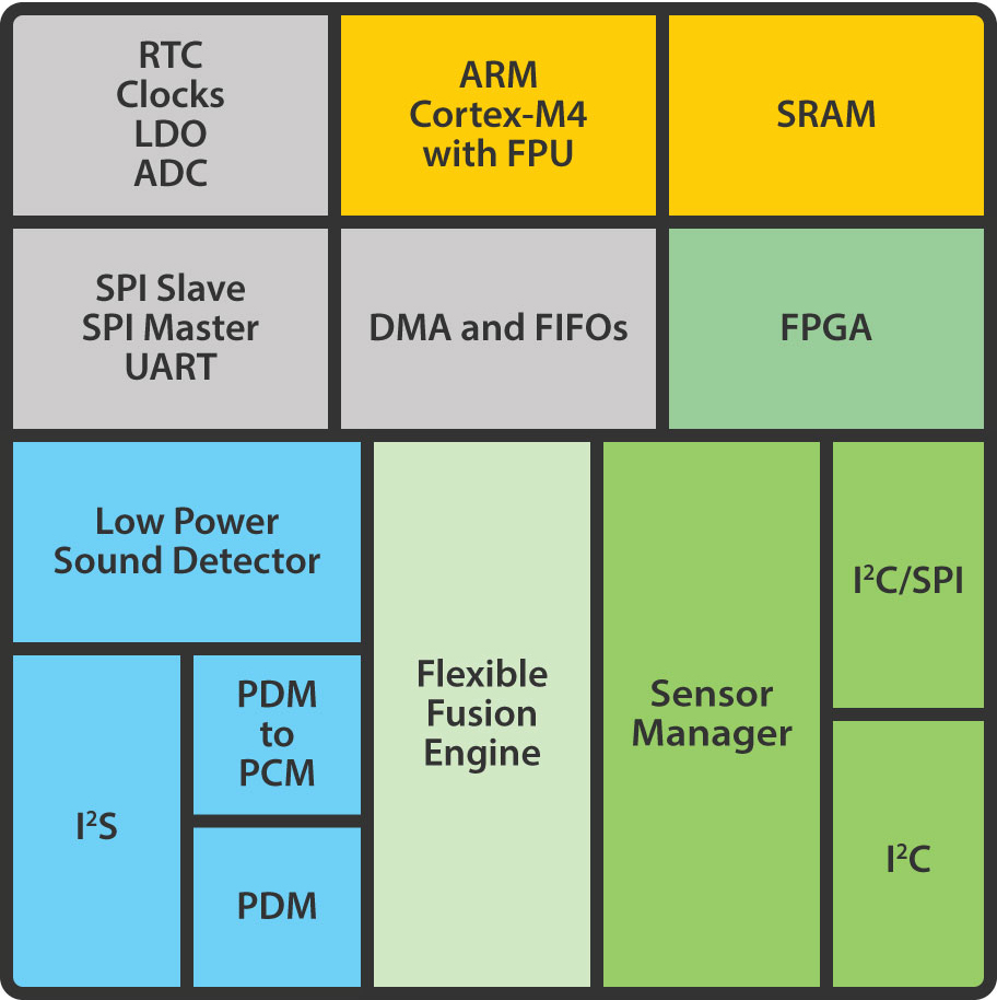
`(Image courtesy Quicklogic)
Summarizing the new elements in the block diagram:
- The blocks in yellow are for running general-purpose software and an OS if desired. Because both phones and wearables are likely to have large amounts of external flash (for things like data logging), the EOS has no embedded flash. The 32-bit CPU (with floating point unit) runs up to 80 MHz; power consumption is 100 µW/MHz or 80 µW/DMIPS. Contains 512 Kb of SRAM.
- The blue blocks are for always-on voice detection. They handle only the first part of voice activation, where the system decides that a sound may be a voice. This is well- enough known to cast into hardware for lower power; higher-level decisions and command parsing would be handled by software either in the EOS’s Cortex M4 or by an external processor.
- The gray portions are system support blocks – including an LDO, which means the device doesn’t need an accompanying power management IC (PMIC).
The audio subsystem, all implemented in hardware, bears further discussion. The different formats and interfaces can get a bit confusing for those of us with less audio background, so here’s an attempt at a Reader’s Digest Condensed version.
Audio is typically digitized in microphones into one of two formats: pulse-density modulation (PDM) or pulse-coded modulation (PCM). The latter is actually probably more familiar: it’s simply a set of integers representing the digitized audio, with framing (so you can tell where the integers start and stop). An I2S bus is typically used to connect audio components using this format; higher-level processing and codecs (used for things like echo cancellation, beam forming, etc.) typically expect PCM.
PDM indicates a value based on how many transitions occur within a given timeframe. It’s a stream of pulses with no framing, and it’s typically carried on a two-wire bus (data and clock). Stereo sound can be carried on one signal, with the left channel sampled on one clock edge and the right channel on the other (although, at present, EOS supports only a single channel).
Some microphones can generate PCM; others (typically cheaper) generate PDM. So this makes possible the following EOS scenarios (which assume higher-level processing is implemented on a different device; the EOS internal Cortex M4 is an alternative for all of them):
- A PDM microphone is connected to EOS; it’s converted by EOS to PCM, and if the voice detector triggers, then the PCM signal is forwarded out the I2S bus for higher-level processing.
- A PCM microphone is connected via the I2S bus. If voice is detected, then the higher-level processor is alerted, and it consumes the signal already on the I2S bus.
- A PCM microphone is connected via the I2S bus; if voice is detected, then the PCM signal could be sent back out onto the same I2S bus using a different channel (since an I2S frame can contain several channels; the drawing below illustrates the original microphone signal on Channel 1 and the forwarded signal on Channel 2). The higher-level processor would need to know to listen to the appropriate channel. This would appear to have no advantage over scenario 2 unless the PCM stream were somehow modified by EOS.
- A PCM mic comes in via the I2S bus; if voice is detected, then the (presumably modified) PCM stream is sent back out onto a separate I2S bus that connects the higher-level processor. The EOS supports two I2S busses.

(Some drawing elements courtesy Quicklogic)
These different options mean that the EOS can be used in a device with a codec, like a phone, or without a codec, like a wearable. They’ve partnered with Sensory for many of the audio functions (hardware and software libraries for execution on the M4).
On a separate note, you may recall that some of the sensor fusion functions in the ArcticLink library came courtesy of Sensor Platforms – which has since been acquired by Audience. QuickLogic decided that they needed a bit more control of their own code, so they hired a substantial team to build libraries internally. That was made a bit easier by the fact that Sensor Platforms kept their code close to the vest, meaning that QuickLogic wasn’t contaminated – meaning they didn’t need to do a cleanroom project.
Of course… now they’re in the same boat with Sensory…
You can get more information from their announcement.


