

If you’d tried to start a power-related conversation with me just a few short years ago, I’d probably have shrugged my shoulders in disinterest. These days, however, it seems the subject of power is on everybody’s lips. It’s a hot topic, if you’ll forgive the pun (and even if you won’t).
I remember the mainframe computer we were working on in 1980. This bodacious beauty consumed 2,000A at 5V. We thought that was a lot. We were such innocents. We didn’t have a clue about the horrors to come.
Just to provide a starting point for our conversation, to ensure we are all tap-dancing to the same skirl of the bagpipes, consider an AI accelerator card as illustrated below.
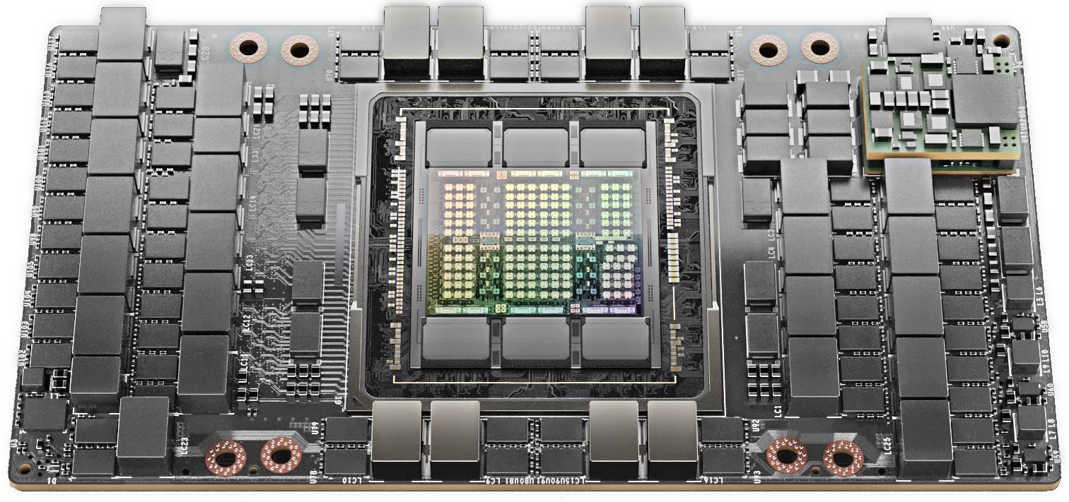
H100 accelerator card (Source: Nvidia)
This is, of course, an H100 accelerator card from Nvidia. The H100 GPU itself is the large square package in the middle of the board. This package contains the main 814mm2 silicon die boasting around 80 billion transistors, along with six HBM stacks.
The GPU occupies only about 25% of the accelerator card’s real estate. With the exception of the small green module in the upper right-hand corner, the rest of the board is filled with DC-to-DC regulators and inductors. Meanwhile, the area under the H100 on the back side of the board is occupied by a sea of ~500 surface-mount capacitors.
Basically, in a crunchy nutshell, 75% of the board is devoted to supplying power to the GPU in the middle. This scenario applies to just about every accelerator card on the planet. Whether the processor (let’s call it an XPU) in the center is a CPU, GPU, NPU, TPU, FPGA, or a custom AI ASIC, nearly all high-end data-center accelerator cards follow the same physical and electrical design pattern.
OK, we are no longer going to discuss the H100 GPU or its associated accelerator card specifically; instead, let’s just keep this overall concept in mind. Purely for the sake of discussion, let’s assume an XPU with a core voltage of 1V that consumes 1,000W. Since P (power in watts) = V (volts) * I (amps), this means we now have 1,000A to deal with.
Many XPUs already have core voltages of 0.8V and 0.7V, with 0.6V, 0.5V, and even 0.4V predicted in the future. As the core voltage falls, the current rises. As more logic dies are added to the XPU, the current rises. Actually, pretty much whatever we do, the current rises. As a result, people are talking about accelerator cards flaunting 1,500A, 2,000A, and even 3,000A in the not-so-distant future.
The concept of surrounding the XPU with DC-DC converters to deliver power across the PCB surface is known as “horizontal power delivery.” This is horrible for many reasons. For example, the power dissipated in the traces—that is, the “loss” in terms of wasted energy or heating—is P_LOSS = I2 * R. To put this another way, the losses increase quadratically with current. And to put this another way: “Eeek!” (and I mean this most sincerely).
Also, since the regulators are so far (relatively speaking) from the XPU, they cannot respond quickly to voltage fluctuations. Where do these voltage fluctuations come from? I’m glad you asked. The aforementioned current draw is not smooth; rather, it’s extremely bursty. This is because millions or even billions of transistors can switch at the same instant when a clock edge ripples through a major logic block, causing sudden current surges that pull the supply rail down, creating voltage droop.
To prevent these momentary dips from crashing the processor, designers must “guardband” the supply—running it slightly above the theoretical minimum to ensure the chip stays above its safe operating voltage. But now we run into another issue: the dynamic (switching) power of CMOS logic is a function of the square of the voltage. This means that if we add a 0.1V guardband to a 0.7V core voltage, this increases switching power by roughly a third because of the V^2 relationship (or the “Eeek2” relationship, if you will).
I was just thinking of Winston Churchill’s speech in the House of Commons on 11 November 1947 (as you do) when he famously stated, “[…] it has been said that democracy is the worst form of Government except for all those other forms that have been tried from time to time.” Similarly, although horizontal power delivery is a horrible way to deliver power, it was the only game in town, until…
Since the beginning of this year, I’ve been exposed to a wide range of power-related concepts and technologies. For example, in a It’s a Mad, Mad, Mad, Mad 48V World we discovered how many of our electronic systems (communications, computing, automotive, industrial, etc.) are transitioning from 12V to 48V. Disrupting AC-DC and DC-DC Power Delivery from Data Centers to the Edge, we were introduced to AC-DC and DC-DC converters that dispense with components like bridge rectifiers, electrolytic capacitors, and inductors, and replace them with small, cost-effective solid-state equivalents.
A little closer to home in the context of our current column, we’ve been exposed to a variety of technologies that aim to migrate from traditional horizontal power delivery to vertical power delivery, moving the power delivery inwards (toward the center of the board) and upwards (into the accelerator board itself).
In Next-Generation Power Technology for Data Center Accelerator Cards, for example, we were presented with a way to remove the inductors and capacitors that consume so much valuable real estate, and to embed them in the board or XPU package substrates, thereby paving the way for vertical power delivery, whose much shorter tracks dramatically reduce IR losses. And in Need 3,000A to Power Your Next-Gen XPU?, we were introduced to the idea of merging the capacitors, inductors, and high-speed switching logic into monolithic DC-DC converters that can be mounted on the back side of the accelerator card directly under the XPU.
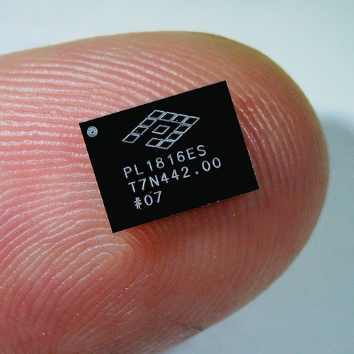
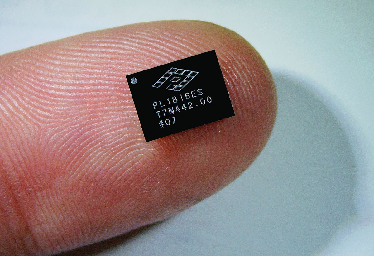
Now, one company is taking all this to the next level. I was just chatting with Dr. Peng Zou, who is the CEO and President of PowerLattice. The company’s claim to fame is its power delivery chiplets. I’m not sure of their exact X-Y dimensions, but they are teeny-tiny, as shown in the image below.
Power delivery chiplet (Source: PowerLattice)
Also, Dr. Peng told me that the “chiplet’s Z (height) dimension can be thinned down as needed, achieving a thickness in the low-hundreds-of-micrometer range. This means these chiplets aren’t mounted under the main accelerator card; instead, they are mounted directly on the XPU substrate within the XPU package, as illustrated below.
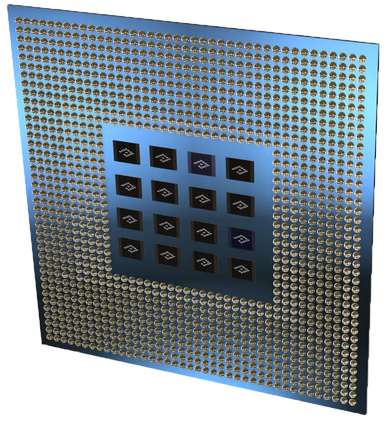
16 power delivery chiplets as part of XPU package (Source: PowerLattice)
Each of these chiplets can handle 200A sustained and 250A peak. This solution is scalable in multiple dimensions. For example, in addition to mounting multiple chiplets inside an XPU’s package, each chiplet is itself composed of many small cells, which means this technology could wend its way into all sorts of devices in the future.
In addition to switching and control logic, these power delivery chiplets also include capacitors and inductors fabricated within the monolithic device, thereby freeing up vast amounts of real estate on the accelerator card for other devices and functions.
But the real “nitty-gritty,” as far as data center operators are concerned, is that XPUs and accelerator cards using PowerLattice’s power-delivery chiplet technology consume only 50% of the power required by today’s solutions.
When you shave 10% off a data center’s power draw, people cheer. When you hack 50% off, they start building statues in your honor. PowerLattice’s power-delivery chiplets don’t merely tidy up the accelerator card or reclaim some PCB real estate—they change the economics of AI. For example, it’s not hyperbolic to say that cutting total XPU power in half pushes back the necessity for new substations and the grid upgrades needed to support the next generation of AI build-outs.
I, for one, am very excited by this, but it’s not all about me (it should be, but it’s not). So, what do you think about all of this?


Next stop, figuring out the power integration into the required memory for those same devices so it stops affecting the rest of the industry.
I’m still waiting for the golden goose of memory technologies — the speed and ease of use of SRAM coupled with the capacity of DRAM and the non-volatility of FRAM — all while consuming almost negligible power… one day…