


“I have a memory like an elephant. I remember every elephant I’ve ever met.” – Herb Caen
When Micron first told me about their new 176-layer flash memory, I thought I must’ve misheard something. That’s a typo, right? Surely you don’t mean you’ve made a chip with 176 mask layers. How heavy is that thing?
Turns out it’s true. Micron has gone up, not out, in an effort to increase the density of its flash memory chips. The company compares its work to the Burj Khalifa versus the Eiffel Tower. And the parts are even shipping today, although Micron is secretive about where.
To be clear, Micron isn’t the only company making (ahem) vertically integrated flash chips. This isn’t even Micron’s first foray into 3D flash. But the new 176-layer device is the tallest, densest flash in production, and it marks a pivot point in the company’s strategy following its cooperative split from Intel.
Logic circuits like microprocessors and Ethernet controllers tend to spread outwards like suburban tract developments. They’re built in two dimensions, which is why die sizes get so big. It takes a lot of real estate to house the 19.2 billion transistors in a Ryzen 5900. But memory chips need to be smaller, widthwise, because we treat them like commodities and pack them in tight arrays. It makes sense for memories to be more like Tokyo and less like Levittown. Assuming you can make the architecture work.
NAND flash memories are basically composed of strings of connected transistors, not too different from logic chains. But really large-capacity memories lead to really long chains with really big chips, long wires, and slow speeds. Flipping the chain into the vertical dimension makes the chip smaller in the X and Y dimensions but thicker in the Z dimension, meaning more mask steps and lots of vertical wires and vias. It’s not a trivial change, but most of the world’s flash makers have now switched to 3D flash.
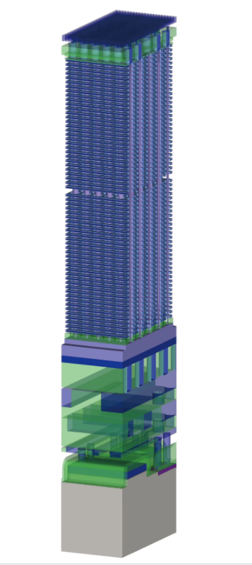
In Micron’s case, there are 176 transistors in the string, all aligned vertically like a 176-story building. Micron’s previous generations of 3D flash had 128 layers, 96 layers, and 64 layers before that. The concept isn’t new, even if the process itself is cutting-edge.
The memory array is created in two “decks” of 88 layers each (visible as the slight gap halfway up the stack in the CAD drawing above). The digital interface logic occupies the ground floor, a technique the company calls CMOS under Array (CuA). It’s all a single monolithic die, not a stack of multi-die modules.
I spoke with Mark Helm, a Micron Senior Fellow, 25-year veteran of the company, and one of the architects of the new flash technology. He said that flash memory design and fabrication used to follow the same path as logic processes (i.e., Moore’s Law) from one process node to the next. But that gravy train ran out of steam at around 16nm. At that point, the gates and wires were too small for the relatively high voltages that flash programming requires. Nonvolatile storage also depends on subtle materials characteristics, and those just don’t scale down to really small feature sizes. It was time to redesign the entire storage cell architecture and go vertical.
On the plus side, it meant that Helm and his colleagues could once again design “fat” transistors that were better suited to storage instead of logic. “We backed up our transistor size by five or six generations” after going vertical, he says. “At 16nm, we could literally watch one single electron move on and off the storage node.” It’s hard to argue that you’ve reached a fundamental limit when you’re down to manipulating individual electrons. Time for a new approach.
In NAND flash technology, storage transistors are organized into cells, with a one-to-one correlation between transistors and physical bits of memory. Over time, cells and the way they’re accessed have morphed from a single bit per cell to multiple bits per cell. Single-level cells (SLC) are now the domain of low-end flash chips. Higher-capacity NAND arrays now store two, three, or four bits per cell, known as a multilevel cell (MLC), triple-level cell (TLC), or quad-level cell (QLC), respectively. Micron’s 176-layer structure is compatible with either TLC or QLC.
Micron isn’t saying where you can buy its newest creation. The company allows that the chips appear in “some Crucial-branded SSDs,” but not which ones. (Micron owns the Crucial brand.) By burying the new devices inside retail products, Micron is giving itself time to ramp up yields and to hide any interruptions in production. The SSD interface can also mask a lot of technical difficulties or teething problems. In the worst case, Micron could conceivably halt production entirely while still producing SSDs and the world would be none the wiser. Unless you decapitate the chips inside your SSD, there’s no way to know whether you’re getting the new 176-layer flash or some other type.
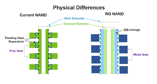
This is Micron’s fifth generation of 3D NAND flash and its second since the end of its cooperative agreement with Intel. That deal ended two years ago, after the two companies had jointly developed 48-, 64-, and 96-layer devices. Those all used floating-gate technology, where the transistors in each storage cell are isolated from their vertical neighbors (hence, “floating”) by an insulating layer of silicon dioxide. Following the split, Micron switched to a replacement-gate, or trap-charge, structure for its 128-layer and 176-layer devices. The company says this as “an interaction-free structure” using silicon-nitride (SiN). The result is less cell-to-cell capacitance – a good thing.
It might be a while before we know when these devices will enter volume production, or when we can buy them as individual parts, or what pricing will be, or what’s inside that SSD. But isn’t that true of all Christmas presents?

