


ANSYS has recently released version 17 of their tools, simply referred to as ANSYS 17. The improvements they made cover a lot of ground, much of it having to do with mechanical design. Which might lead you to think, “oh, this is a mechanical tool; I can move on, since it’s not for me.” But be not so hasty: we’ll return to this in a minute.
Their theme for the release is 10x, meaning lots of things are 10x better. 10x is a convenient number (I personally think of it as a convenient threshold for how much better something needs to be to get a user to switch from something else). Again, this distributes over so many feature changes (many of them mechanical) that we could take all day chasing that angle. But suffice it to say that many of the changes aim to smooth or unify flows and, in general, save time and effort.
The conversation I had with them focused on but one aspect of the upgrade, and it’s one that is relevant for chip and board designers –on both the mechanical and the electrical side. The capability implications are nominal, but the flow implications are more substantial. In addition, our discussion raised a question about encrypted silicon IP, so we’ll address that as well.
Stressed out
The first area we’re going to look at is the ability to assemble a model of an entire board, from chip through package to board. And, to hear ANSYS tell it, the status quo has involved two silos: the electrical one and the mechanical one. The specific problem they’re focusing on is the ability to model the stresses caused by the heat put out by high-performance chips.
The scene they describe is one where the electrical team will provide the mechanical team some data about the chip they’re using. The mechanical team will then go off and model the thermal behavior and give the electrical folks some temperature data that can be used for corner simulations back in the electronic world.
And, to be clear, each side is using a different set of tools and models. I mean, let’s face it; mechanical guys have greasy hands from working with actual stuff, right? Don’t want to risk getting grease on the delicate, pristine electrical models, would we? Ick!
But, in fact, this is not an efficient way to go about business – tossing data back and forth across the wall. And so one aspect of ANSYS 17 is that a single unified model can be worked on one side by electrical folks and on the other by mechanical folks.
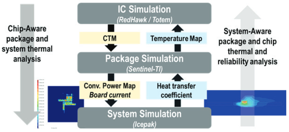
Image courtesy ANSYS
That makes not only for a unified model, but also a unified tool, since it’s made for use by both sides.
There’s another piece of this, however, that required work before the full-system stress analysis problem could be considered solved. It’s great to talk about doing a system simulation that includes the board, package, and chip; it’s quite another to execute those calculations. In fact, they say that a full finite-element analysis solution would be prohibitive.
So they applied a solution that they’ve already used for thermal analysis – except that they had to modify it because heat flow and stress doesn’t. They now do a pre-processing step that takes each layer of the PC board and creates a model, determining the “metal fraction” of the layer. This makes the analysis easier to solve (although I would assume they can’t ignore the location of the metal, since metal in the right place would help to wick away heat and reduce stress; metal somewhere else wouldn’t).
The secret key
The other aspect of this release stimulates a topic less about ANSYS than about other tools. It relates to how you build a model of a system using intellectual property (IP). IP models in the electronic space have been protected by encryption for several years now; such protection is a popular feature. Until this release, such model encryption hasn’t been available for mechanical models. ANSYS has included 256-bit AES encryption in this version.
Within the context of this chip/package/board simulation problem, it would appear that detailed models of leadframes and packages and such are considered IP by their purveyors. This makes it harder to get models (or makes them more reluctant to release any such details). Once encrypted, however, you can plug the pieces together and let the tools handle the calculations away from human prying eyes. Of course, it also works for other mechanical modeling far from the semiconductor realm.
This got me wondering, on the heels of our recent discussions of IoT security and encryption, how keys are managed with IP models. Given Synopsys’s role in this whole thing, I had a conversation with them to understand this better.
Here’s the issue. The encryption is now done using AES, which uses a symmetric key system, meaning that you use the same key both to encrypt and decrypt the model. In most such systems, if you have multiple tools or models or systems or whatever that use this key, then they all use the same key. That means that if you crack one key, you have them all.
The obvious alternative is to create a different key for each model. But then you need to ship the key with the model so that the tool can unencrypt the model. This has obvious security implications, since anyone who can crack the message with the key gets the key. There are also further complications if, for example, you have multiple instances of a single model or multiple projects using different instances of the same model – when those instances have different keys. (This happens in particular with public/private keys, which Synopsys tried for a while until it proved too cumbersome.)
So how could this work? Turns out this isn’t a stupid question and the solution is surprisingly involved. In fact, each model gets a different key, and the key is transmitted – within the model. Here’s how it works.
First, a seed is used to stimulate several rounds of randomization and hashing and trips through a trap-door (a one-way function that’s easy to calculate but hard to reverse). From this they get a key. That key is then encrypted and hidden within the model. Not like, if you look you can find it, but rather they break it up and scatter it throughout the file, somewhat like a photo watermark. The locations can be different each time, so the scattering algorithm is intended to be hard to crack.
When a user receives the model, the tools can go in and find the key (since it knows the algorithm). Except that the key is encrypted – how does it know the key-to-the-key? Turns out that this key key is also algorithmically created by taking a seed and randomizing and hashing etc. But the trick is that each release version has a different seed. That seed, when “randomized,” is actually run through a pseudo-random number generator. Emphasis on “pseudo.” In other words, it’s deterministic.
So if the model-generating tool and the model-using tool both know that algorithm, then from the same seed they’ll create the same key. The seed changes with each release. Keys created on older versions will work on newer versions; keys created on newer versions will not work on older versions. (Remember, this isn’t the key to the IP, this is the key to the key buried within the IP).
So, to summarize, the key to the model is transmitted in a way that’s very hard to find. The key to the key is determined algorithmically at both ends (generation and use) so that there’s no need to transmit it.
As another protection, if any of the files have been altered by even one bit, they won’t run. This means that you can’t go in and start experimenting with a file to figure out the algorithms. And this really is about the algorithms – there’s the IP key generation algorithm, the bury-the-key-in-the-file algorithm, and the key-to-encrypt-the-key algorithm. You’d have to crack them all to break the system. (Or at least that’s the intent…)
So, all of this is why you can receive an encrypted model from your IP provider and never have to worry yourself about unlocking the thing; it simply happens automagically.
For any mechanical folks on here, I did check with ANSYS to see if they operate the same way; as of pub time, I haven’t received an answer.
Again, there’s lots more going on in this release than we can cover here; I refer you to the link below to dig deeper.
More info:


What do you think about ANSYS’s approach to chip/package/board stress analysis and Synopsys’s approach to IP encryption?