OK, folks, time to get out the copper polish and the soft cloth. We’re going to dress up the metal that adds a patina of shiny to our work. (OK, patinas often aren’t shiny, but you can forgive a tarnished metaphor, can’t you?)
Things are happening in the world of metal. And three of those things are topics for today. They come to us from Applied Materials (AMAT) and Imec. And we’ll take them in that order.
A Difficult Hardmask
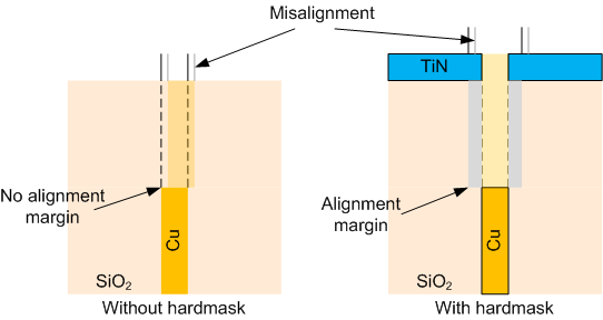
The first involves metallization, although the material of interest isn’t a metal per se – it’s a hardmask. It’s put there to help with via alignment. The thing is, especially when using a via to connect to a lower thin line, you want the via as wide as possible (for low resistance), perhaps as wide as the line. But if you try to achieve that by printing a via of that width and hoping you align perfectly, you’ll probably come away disappointed.
Because such an arrangement provides no margin for misalignment. And there will be misalignment. And when that happens, part of the via will contact oxide, which isn’t particularly useful. On the other side of the via landing, some of the line metal will remain uncontacted. Result? A thinner-than-planned via (effectively), meaning higher resistance. In the simplest case (pictured below), there is no margin for alignment errors.
The traditional fix for this has been to use a hardmask for a so-called self-aligned via. Hardmasks are made out of a material that can be etched, but not with the chemicals or methods used to etch SiO2 (or some other material to be masked). So it can be patterned by etching, but then it acts as a mask when the oxide is etched. And it can then be removed.
What this allows is for an opening in the hardmask to be patterned above the metal line. The via can then be oversized so that, even if it’s shifted a bit one way or the other, the hardmask ensures that the full complement of metal contacts the lower copper line.
Now, if you’re still awake, you may notice that this really hasn’t eliminated an alignment problem; it has simply moved it. The via alignment problem is gone, but it’s replaced by alignment of the hardmask opening above the metal line. According to AMAT, this alignment is easier to manage than the via-to-line alignment is. So we’ve traded a hard alignment issue for an easier one.

This isn’t news. AMAT says it’s been around since the 90-nm node. And the preferred Hardmask material has been TiN. But, as we continue to scale down, problems are creeping up with TiN as currently deposited. There are actually two issues: density and strain. And they affect each other.
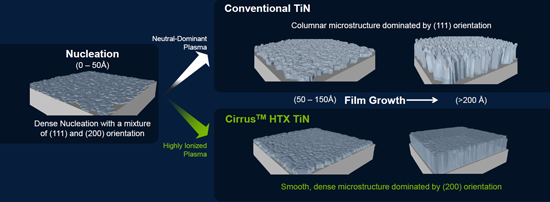
It would be ideal if the perfect bulk density of TiN could be attained when it’s deposited on the wafer. That would be 5.5 g/cc. But the deposition method, physical vapor deposition (PVD), isn’t perfect. For the first 50 Å, the TiN layer grows in a manner more or less insensitive to how it’s deposited, with a mix ofandcrystal orientations.
It’s at that critical 50-Å position where things get funky. Using traditional PVD favors growth along theorientation, resulting in pillars with voids between them that are hard to fill. So the traditional approach is to crank up the ion energy at that point and smash the crap out of this layer to force ions into the voids and, effectively, tamp down the material to pack it. This process gives the layer compressive stress, with density at about 4.5 g/cc.
At this point, it helps to note that we are now in the era of low-? dielectric. This has lots of voids (part of what lowers the ?), but it also makes it softer and more subject to being pushed around and distorted. Given a compressive TiN layer, narrow lines or vias tend to buckle and bend – an effect not noticeable with wider lines.
So you really don’t want this compressive layer. In fact, if TiN were to grow “naturally,” its tendency is towards tensile stress, not compressive. The compression comes only from the ion bombardment. The challenge, then, is to deposit a tensile layer of TiN.
AMAT claims to have accomplished this with their Cirrus HTX unit, and here’s how they describe what happens. Given a higher ion concentration,growth is favored overgrowth. This requires careful ion concentration and energy control and the ability to vary it in real time during deposition. In addition, by heating up the wafer, ions can migrate around the surface to find lower-energy places to settle.
(Click to enlarge. Image courtesy Applied Materials)
The result is a tensile layer with density 5.4 g/cc – almost as high as the bulk density. And their results show much straighter narrow lines than is possible using conventional deposition. This may allow this hardmask approach to extend even into the 7-nm node.
(Click to enlarge. Image courtesy Applied Materials)
One question I raised was whether there might be a material other than TiN for the hardmask. There may or may not be, but the preference is strongly for sticking with TiN, since it’s well known. Changing that would involve many more changes in the overall production line, and, frankly, no one relishes that prospect. So as long as they can extend TiN, they’re going to.
More Filling
Meanwhile, Imec did some work with Lam Research investigating the use of electroless plating instead of chemical vapor deposition (CVD) for filling vias and contacts. The issue here is higher-aspect-ratio (that is, tall and thin) holes – and filling them without voids. As the vias get taller and the contacts get thinner, it gets harder to fill them uniformly. At the small sizes that matter here, voids can cause a measurable increase in via resistance at best and problematic decreases in yield at worst.
So-called electroless plating isn’t new; there are many other places where it’s used, but they’re generally in the macro world. Its name comes from the fact that it’s a plating technique that doesn’t involve the usual electric field that biases ion movement in standard plating. You could imagine that having to bias every via bottom in a chip for plating purposes might prove problematic.
The nice thing about the process is that the chemistry involved automatically makes it selective. A metal surface (Cu, Rb, or Pd in particular) catalyzes the reaction, making it possible to fill (or pre-fill) vias with cobalt using no barriers or liners. If tungsten is underneath, they found it beneficial to use a monolayer of palladium as catalyst to protect the tungsten from dissolving.
The trick is to prepare the bottom of the holes properly to eliminate oxides and other impurities that would get in the way. The sidewalls must also have an adhesion layer, although there will be no nucleation on the sides. This is a wet process; the wafer is literally dunked into a iiquid. Proper preparation ensures that all the necessary surfaces will be wetted and that tiny air bubbles (which you could imagine getting stuck inside a tiny via) won’t be a problem.
They see this as benefiting interconnect at the 7-nm node and beyond.
Take it Direct
Our last topic opens up the possibility of etching copper lines directly as an alternative to the “traditional” damascene process. For me, this prompted an internal, “Whoa whoa, wait just a doggone minute here…” moment.
See, I was more directly involved with this sort of stuff when aluminum was the interconnect of choice. I then moved to the dark marketing side and was preoccupied with being evil, so I missed the transition to damascene. To me, that meant that direct etch was “traditional” and that damascene was the novelty needed to solve some problem with direct etch. Or else we would have stuck with direct etch the whole time.
So here we are, blithely returning to direct etch, which raised the obvious (to me) question: “If direct etch didn’t work before, why is it suddenly going to work now? What’s changed in copper to make this feasible?”
The original problem with etching copper was that the plasma etching process that had been used for aluminum wouldn’t work on copper. And, according to Imec, what’s changed is mostly that the copper layer has gotten much thinner. As we’ll see, further details are still blurry.
But with that elephant in the room acknowledged, let’s get back to the problem here. Way back when, we transitioned to dual damascene, but, as we scale the lines smaller and smaller, we’re having a real issue with line resistance.
It turns out that one of the contributors to this problem is the copper grain size: the damascene process results in small grains, and the grain boundaries increase resistance. What Imec did was instead to deposit a blanket of copper over a TaN/Ta barrier, resulting in larger grains and lower resistance. This layer was then etched in the way aluminum used to be, although there are details to exactly how the etch was done that have not been included in the paper; they’re considered proprietary. So it seems fair to assume that, while the copper etch resembles the old aluminum etch in a general way (as compared to damascene), the specifics are different.
The copper is topped off with a SiN layer to keep the copper from wandering all over the die, as it is otherwise wont to do.
This makes possible a return from damascene for future nodes. A lot of work went into making damascene work; presumably it will take work to adapt direct etch to fleeting modern dimensions. But keeping line resistance low is critical to scaling; moving back to direct etch may be just what’s required.
More info:
Applied Endura® Cirrus™ HTX PVD
Both Imec papers were presented at IITC; I have found no online proceedings with links to the papers. Please contact Imec or IITC for more information. The paper titles are:
“Cobalt Bottom-Up Contact and Via Prefill enabling Advanced Logic and DRAM Technologies,” Marleen H van der Veen et al
“Direct Etched Cu characterization for Advanced Interconnects,” Liang Gong Wen et al.


So thinner copper is able to be etched like aluminum but the thicker copper of yesterday was not? What gas are you using to etch the copper today? According to http://www.plasmaetch.com/plasma-etching.php you can etch AL but not CU?
I’ll see if I can get a more detailed response out of Imec. I suspect the qualification is with “just like Al” – that it can be etched just like Al can be etched, but they’re doing something different that they’re not disclosing.
I just had a follow-on conversation with the Imec gentleman and got a bit more info, although not everything.
According to him, the primary reason for switching to damascene in the first place was etch rate: with 1-um or 500-nm layers of copper, it simply took so long to etch that it wasn’t economical.
The thin films they’re targeting today are 20-60 nm. So even with the original slow etch rate, this becomes more tolerable. That said, apparently the etch rate has also been improved somewhat, although my sense is that this isn’t about a revolutionary new etch process. Even so, he wouldn’t reveal details about etch chemistry or recipes.
Hope this helps…