

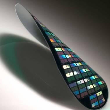
For some years, when I have travelled, my passport has been stowed in my hip pocket. This has worked well (apart from the incident with the cool wash cycle) but did mean that my passport developed a firm curve. Earlier this year I needed a new passport, and when it arrived, there was a firm instruction: “Do not Bend”. This is, presumably, because it has a chip inside, and, as we all know, silicon does not bend. But when you talk to, among others, Gerhard Klink of the Fraunhofer Institute’s “Group Polytronic Technologies” in Munich, he can show silicon bending. It is easy, really. You start with a standard wafer, build up your circuit on one side, and then remove the back side of the wafer mechanically until you achieve a thickness of less than 25 microns. (The technology for making wafers thinner has been well developed for MEMS sensors and related products.) At this thickness, it is possible to bend silicon easily.
Why would you want to? Apparently, the makers of smart cards are looking at this. Many of you in the United States may not be aware that most credit cards in the rest of the world have an integrated chip, and, instead of swiping a magnetic strip through a reader, a transaction involves a conversation between a card reader, the card, and the card user. The card owner enters a PIN (Personal Identification Number), which is checked by the card reader. Chip and PIN technology is inherently more secure than magnetic stripe reading. (And it is coming to the US this year – possibly.) Other smart cards are used in such things as pre-paid multi-use public transport tickets, usually with Near Field Communication (NFC) built in. Since plastic cards naturally flex, having chips that flex as well provides obvious advantages. Although Fraunhofer is working with major smart card companies and their silicon suppliers, smart cards have been around for some time without using flexible silicon.
But firstly, what is the Fraunhofer’s “Group Polytronic Technology”? It is part of the Fraunhofer-Gesellschaft, which is, according to their web site, “… Europe’s largest application-oriented research organisation. Our research efforts are geared entirely to people’s needs: health, security, communication, energy, and the environment.” Fraunhofer has 24,000 people, most of whom are scientists and engineers. It has a budget of Euro 2 billion, (US$2.8 billion) of which Euro 1.7 billion comes from contract research. As well as industry funding, there is also funding from the German Federal Government and from the Länder (the Länder are the German equivalent of the States in the US). A significant and growing part of the income comes from licences for Fraunhofer-developed technologies. The 66 Institutes and research units are organised in 7 groups, one of which is Microelectronics. Within this group is the Fraunhofer Research Institution for Microsystems and Solid State Technologies EMFT, based in Munich, and part of this is Mr. Klink’s Group Polytronic Technology.
The group has two technology areas: Silicon Wafer Processing (particularly MEMS technology) and Plastic Film Processing (particularly reel-to-reel technology).
While flexible silicon still looks a little like a solution in search of a problem, plastic film is a fascinating technology, or rather a fascinating range of technologies. With plastics, we are looking at organic materials – carbon-based electronics – something that has been a research target for many years. The first breakthrough came with OLEDs (Organic Light-Emitting Diodes).
OLEDs use electroluminescence – a phenomenon that was first recognised in the 1950s and has taken well over 50 years to get to volume commercial exploitation. If you put a current across some organic molecules, they give off light. Which of the millions of organic compounds to use to get reliable light, how to get the light in red, green and blue to allow full colour, and how to manufacture this in volume: all these are what have been difficult and the reasons why it has taken so long to reach production, but today there are tablets and phones using OLED in quantity.
While most of today’s displays are on glass substrates, there is considerable interest in using thin plastic film as a substrate. The main drivers are not primarily related to flexibility but instead are lower weight, greater resilience, and low power. In one particular area, E-readers, a plastic film technology is dominant. Most E-readers use the Pearl display technology from E Ink, an MIT spin-off. The working element is a capsule containing oppositely charged particles of black and white pigment. Applying a charge to the back of the capsule attracts one set of particles and repels the other. Removing the charge leaves the image stable, and reversing the charge flips the particles. Power use is very low, and you are reading from a reflecting surface, so you need no other light source. Neat! These capsules are embedded in a film, using a reel-to-reel process, at around 1200 pixels per square inch. (Sorry – reel-to-reel is a process wherein a reel of material unwinds to be fed through the process steps and then is either re-wound onto another reel or sliced into sheets.)
It is this technology, with low cost production, low power consumption, and low weight, that first made E-readers economic, and it is why, despite the possibility of reading on other media, E-readers are still selling in quantity. However, the process is poor for colour and doesn’t give a true white – more a very light grey.
If you print on plastic film with a conducting ink (silver-based inks are currently the favourites, but other forms are being sought), you can create circuit elements, such as capacitors, resistors and even transistors. Ink jet printing can produce feature sizes as small as 25 microns. Screen printing, with two stages – creating the mask and then printing the circuit – is more complex and can’t yet reach the dimensions of the ink jet screen, but it provides higher throughput. Films can also be coated with sputtering or deposition and then etched like a wafer. Like on a conventional circuit board, it is possible to create multiple layers laminated with other films of different characteristics and with metal foils. Lasers and plasmas can be used to remove material and create through-film vias. In these cases, line widths down to 10 microns are possible.
Local areas of electroluminescence allow the creation of displays and, with thick films, etched cavities can house thin-silicon ICs, including micro-controllers and MEMS sensors. Energy can come from film photovoltaics or from thin-film rechargeable batteries. Communication can be through printed antennas and control through capacitive or resistive sensing.
At this point you should have your imagination running and thinking, “I could build a …”
Some of the imaginative things include labels for goods that can display if they have been subject to shock, or have gone outside pre-set temperature limits. Add an antenna, and the label can be read automatically using NFC.
Displays are another area. The ubiquitous pop-up banner at trade shows and in the retail environment could be replaced by a pop-up that runs video or a PowerPoint presentation. Buses and trains today often use printed vinyl for company liveries and advertising. These too could now run video (although there may be safety issues).
A laptop could consist of two small roll-out sheets, one with touch sensitive areas working as the keyboard, with the other one providing a display. Rolled up, the entire package could be a one-inch diameter cylinder about 14 inches long.
For years, supermarkets have wanted to replace printed shelf-edge labels with a programmable display, but the savings in not having people go round changing labels every day have not been sufficient to repay the investment in displays. With film technology, this looks more achievable.
Around the world, not just at Fraunhofer in Munich, there is a ton of work going into plastic electronics. This has not yet reached the tipping point for large-scale commercial exploitation, but my feeling is that it is only a matter of time. But then, people have been saying that for several years now.


What could you build with a flexible circuit?