


The concept of designing, validating and then reusing functional blocks in integrated circuits (ICs) has been entrenched in the electronics industry for decades. Software development has a similar model utilizing libraries of common function calls or objects. However, the concept of reusing printed circuit board (PCB) modules is much less common. Reusing PCB modules for common or commodity functions offers considerable advantages, for example avoiding potential signal integrity or thermal problems, by utilizing circuit data whose performance has been proven in previous generations of products. The key to successful modular circuit design is a data management system that can store and control access to modular reusable blocks, manage information that is critical to design reuse, such as the layer structure of a routed block, and interface easily with the circuit design software. The end result is a reduction in time during schematic capture and PCB design, along with fewer design errors, making it possible to bring quality products to market faster.
Circuit design challenges
The volume and frequency of new product introductions require new design methodologies. Reuse is becoming a competitive requirement. The size and complexity of today’s electronics products makes it impossible to generate a new design from scratch each time. Instead designs are largely, created by selecting and combining existing blocks of circuitry. The availability, variety and quality of these reuse blocks depends on the company. Some have embraced this new methodology and others have not.
This topic is getting more attention because much of the electronic content in a wide range of electronics products has been commoditized with the consolidation of increasing amounts of functionality in application processors or system-on-chips (SoCs) and their associated reference designs. Along with this consolidation is the standardization of busses and protocols allowing for even more reuse.
Today, circuit designers face challenges such as the increasing density of nets, the proliferation of electrical constraints along with reductions in PCB size – not to mention stricter-than-ever requirements to maintain reliability, electrical response, manufacturability and compliance. IC and field-programmable gate array (FPGA) vendors are implementing serial asynchronous architectures operating at higher speeds than ever, creating new challenges in meeting jitter and bit error rate specifications. The increase in data rates, faster component edge rates and major changes in I/O architecture put additional pressures on circuit designers. An increasing proportion of today’s electronic products require high-speed design techniques to ensure that PCB guidelines and high-speed requirements are met, however, they still need to be produced quickly and inexpensively.
The amount of time and effort required to overcome these challenges is significant. Experienced engineers in circuit design put in time upfront, and then additional effort is spent in simulating circuit performance from a signal integrity, power integrity and thermal standpoint. Often many iterations are required in order to find a design that successfully passes the simulation requirements. The next step is building a prototype of the PCB and performing an exhaustive series of tests to validate its performance. Often additional changes are required during the prototyping phase. Of course, the greatest test of all comes when the product is delivered to the customer and achieves success in the marketplace.
Current circuit reuse methods
When the time comes to produce a related product, such as a next generation replacement or a variant targeted at a niche market, it is common practice to reuse the circuitry in the original design. This is usually accomplished by copying and modifying the original design, or by utilizing predefined modules from the original design. For example, a new cell phone variant might utilize the same baseband, Bluetooth and Wi-Fi modules as the previous design, combined with a new RF section. This is because creating a related product from scratch would take a considerable amount of time and potentially introduce design errors.
Another approach circuit engineers may use is to copy and paste from previous related designs; however this approach has several drawbacks. In larger companies, it can often be difficult to find a related design that fits the specific requirements of the current project. There’s always the potential for the designer to inadvertently reuse a version of a related design that does not include the latest changes and thereby replicate problems resolved in the latest version of the earlier design. Another problem with the copy and paste method is that the knowledge developed in creating the original design is typically lost. The copied blocks lack intelligence such as the underlying design methodology and best practices. The copy and paste approach also lacks traceability. It’s typically necessary to rely on the engineer who created the original design to determine the source of individual modules. If a problem is discovered with the source module at a later date, there’s a good chance that the designers of the new module will not even be aware of the change. In that case, the error that stimulated the original change will crop again and have to be resolved in the copy, hopefully before the product is released to customers.
Managing modular circuit blocks

Fig. 1 Reusable modular schematic and PCB blocks
These problems are being addressed by data management software that stores reusable circuitry in the form of modular blocks, greatly simplifying the process of reusing existing PCB schematics, parts lists and layouts. The new generation of data management software controls access to circuit blocks by providing information only to authorized users and ensuring that only users who are authorized editors are allowed to make changes. To perform changes, a modular block must be checked out. While a block is checked out, other users are prevented from making changes to it in order to ensure the integrity of the block. Furthermore, the data management software can be configured to require either one or a series of approvals when a change is made to a modular block. The modified block is then automatically routed to the designated approvers.
Reusable modular blocks can be created in two different ways – either the top-down or bottom-up approach. The top-down approach involves partitioning the design in the early stages of the design process, creating the block diagram, then adding the appropriate circuitry to each block. When the blocks are validated and the design is completed, the parts list, schematic, and layout of each block is then registered in the data management system along with its metadata. Metadata allows the block to be found easily and contains detail such as which products the block is used in, the engineers involved in its design and the approval chain. Conversely, the bottom-up approach starts with creating and validating the circuitry. After the circuit validation is completed it is then partitioned into blocks.
Overall the top-down approach is usually the most effective, but it does require more time for planning. The payoff is that the blocks produced by this method are typically more suitable for reuse, so considerable time is saved in the design of variants that utilize these blocks.
Streamlining the design process
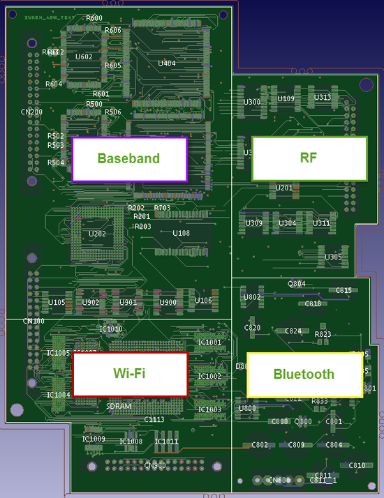
Figure 2 Partitioned designs facilitate circuit reuse
The modular design approach is not a panacea, but it can substantially streamline the design process. Let’s look at how it could be used in circuit design for the cell phone example mentioned earlier. In this case, let’s assume that the predecessor design has been partitioned into blocks representing the RF, baseband, Wi-Fi, Bluetooth and other sections. The engineer working on the new variant can easily call up these modules by searching the data management system on the product name. The engineer can then check the documentation stored in the data management system for each module they plan to use to ensure it is a fit for the new design. Then the engineer can drop the modular blocks that will be used without modification into the new design. The parts list, schematic and layout of each modular block will all be incorporated into the new design.
The engineer can then design the new RF block and any other new blocks needed, either from scratch or by modifying existing blocks. They can then connect the sections together and route the new areas of the design. Next come checks on issues such as signal integrity and thermal management, while focusing on the newly routed areas. Of course it is still necessary to do basic simulation of the complete design because even though we know that each individual block works fine, there’s the small possibility that combining them might cause a problem.
In conclusion, modular circuit design offers a number of compelling advantages that are leading to its rapidly increasing adoption. The ability to share circuit modules across many products and projects can reduce the manpower required for future projects, thus reducing development costs and improving productivity. Test and regulatory compliance time is also reduced through the use of proven design blocks. The reduction in design time makes it possible to bring products to market faster which helps increase revenues and enables new products to gain market share before they face serious competition. Modular circuit reuse also reduces errors by allowing designers to utilize proven designs wherever possible. Now is the time to begin utilizing modular design to enable your teams to increase the speed of developing and releasing boards.
About the Author:
Craig Armenti, Senior Technical Marketing Manager for PCB Products at Zuken USA, Inc.
Craig focuses on working with customers to deliver and implement solutions that provide process improvements and drive the utilization of best practices. Craig has held Application Support and Management positions with several major telecommunication companies. He holds Bachelor of Science in Electrical Engineering Technology and Master of Business Administration degrees.


9 thoughts on “Get to Market Faster with Modular Circuit Design”