


We’re shrinking again. We’re moving past the 20nm node into the 16 or 14 realm (depending on how you or your marketing team counts it). In fact, according to KLA-Tencor, some companies are skipping the 20nm node altogether and moving directly into the teens.
It’s always been the case that new nodes spur new tools, but there are some trends underway at 16/14 that are more than just “smaller,” and they are providing yet more challenges to the semi equipment guys.
Tools for Building
3D NAND probably provides the biggest change, and it introduces a new layer cake onto the wafer. For those of you that are new to 3D NAND, Applied Materials (AMAT) provides a simple description of what it consists of: tipping a string of bits on end.
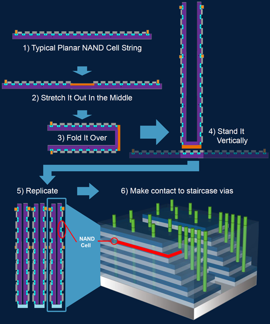
Figure 1. 3D NAND is a planar string halved and folded.
(Image elements courtesy Applied Materials)
Why not simply reduce the cell size? Again? Because we’re pretty much done with that; you’ve got to have some room for trapped charge to inhabit. And you need room for enough charges to be statistically stable. So instead of making the planar string smaller, it’s made vertically. This reduces the horizontal footprint (as you can see from the salmon-colored line by Step 4). The cost of that is in vertical complexity.
You’ll notice that the final result has many thin alternating layers of polysilicon and oxide. Then the holes for the gates are drilled all the way through (in one step, not after each layer – a 60:1 aspect ratio), and they’re concentrically filled with oxide, nitride, oxide again, and then polysilicon. In other words, the gate stack goes horizontal now that the string is vertical, with concentric cylinders in the holes acting as that stack.
These layers are thinner than your average metal/oxide layers for interconnect. And there are lots of them: you think that 8 or more layers of metal is tough – this is 24-32 thin layers, moving to 48 and more. So planarity is critical, as is defect control, since one defect at the bottom of this cake can screw up all of the layers above it.
In addition, the hard mask for drilling the holes has to be of extremely high quality and selectivity. These aren’t just contact or via holes; the concentric rings, forming the gate, need to be pristine, meaning that the drilled hole needs to start out clean. And selectivity is important because, due to the depth of the hole, that hardmask is going to get a lot of abuse before the drilling is done.
Applied Materials is touting a new chemical vapor deposition (CVD) platform for this: the Producer XP Precision.
Meanwhile, both 3D NAND and FinFETs have increased the number of layers that need to be planarized. For FinFETs, for example, we took the following inventory:
- Shallow trench isolation (STI): 1
- Poly FinFET: 1
- Poly open (replacement metal gate): 1-2
- Metal gate: 1
- Self-aligned contact: 2 (to gate and to drain)
- Local interconnect (LI): 1-2
- Interconnect (what we’re already used to)
In other words, chemical-mechanical polishing (CMP), in the past used solely for the back end, has now joined the front end as well to raise the number of CMP steps to something on the order of 20.
What’s interesting here is that they’ve moved from a one-step CVD process to a multi-step process. You might think, “What’s the difference between doing it all in one step and doing it in several steps?” Well, the machine has several stations, and a wafer moves from station to station as it completes the polishing. Each time it takes a break between stations, the temperature comes back down and the waste materials get purged – sort of like changing the bathwater before continuing. They’ve found that this provides a higher-quality result, as suggested below.
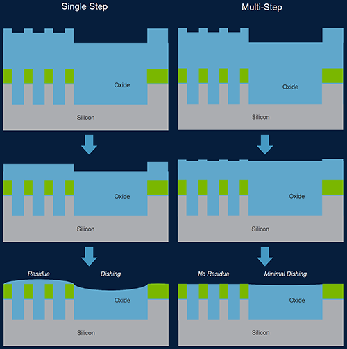
Figure 2. Multi-step CMP reduces residue and dishing.
(Image elements courtesy Applied Materials)
Of course, you wouldn’t want three out of four stations to sit idle as a wafer moves through the steps. This is operated as a pipeline: as soon as a wafer moves from station 1 to station 2, a new wafer occupies station 1. So, during full-on production, all stations are busy. That said, you can still use it sequentially or in a batch mode.
They’ve also turned the platens vertically, which helps with defect management. And in-situ process control helps to improve the quality of the polish.
And Applied’s new machine that does all of this: the Reflection LK Prime. It was introduced along with the Producer XP Precision CVD platform.
Tools for the Building Inspector
Meanwhile, KLA-Tencor has been busy assembling new inspection platforms for these new nodes. As a reminder (since we’ve looked at some of this before), inspection is a dodgy business at these dimensions. For the most part, you’re not actually looking for identifiable defects; you simply can’t see them clearly using machines that provide the throughput needed for in-line monitoring.
So instead, you end up looking for signatures, and different defects have different signatures. You end up playing with various optical “modes” to identify which ones provide the best sensitivity and contrast for a given wafer on a given process.
Even at this level, there are two types of inspection. During process bring-up and for R&D purposes, there are broadband machines that cast a wide net, since some defects are more visible under different wavelengths of light.
But for production purposes, it’s more typical to use a laser scanner. As such, it’s a single wavelength, so again, it’s a matter of selecting modes and figuring out how a given wafer should be inspected.
And finally, once a defect is signaled, you go to a separate review machine to try to identify what the defect is. This requires critical alignment so that the review machine can home in on the offending area.
With all of that in mind, KLA-Tencor has introduced four new machines:
- The 2920 Series: a broadband plasma inspector for patterned wafers featuring twice the deep ultraviolet (DUV) light (brighter than the sun, they say); Accu-Ray and Flex Aperture for quickly figuring out which lens and wavelength modes best identify defects; a smaller pixel and shorter wavelength for higher precision and better signal-to-noise ratio; and new algorithms. They claim to have been able to identify new yield-killing defects in one day.
- The Puma 9850: A laser-scanning inspector for patterned wafers featuring, again, twice the light; a smaller pixel as well as boosted sampling for higher throughput; a “line formation cylinder” for higher resolution; and a variable analyzer and new sensor to deal with noise and boost the signal, respectively.
- The SurfScan SP5: this is the latest version of their DUV inspection system for unpatterned wafers. Those could be raw wafers or, for instance, wafers that have just gone through an epitaxy step and haven’t yet been patterned. This device features more DUV power, refractive optics to preserve light polarity, “optimized spots” for improving sensitivity while keeping high throughput, polarizer masks to filter noise, integrated haze mapping, and a new computer with new algorithms.
- The eDR-7110: a review station for identifying defects. It has improved classification; “chain testing” – if one test doesn’t ID the defect, then it can try backup strategies; immersion optics for better resolution; faster sampling; new “unique” connectivity for getting results faster; and improved defect data.
There’s a subtle message in the SurfScan release, by the way. We talked about their prior SP3 version of this before (there is no SP4, since these get sold a lot in Japan, and they treat 4 like we treat 13, except more seriously). And that model anticipated the new 450mm wafers by including capabilities for both 450mm and 300mm wafers. The SP5: only 300mm. They’re still having a hard time seeing demand, since the cost benefits of the larger wafer haven’t yet settled. In their eyes, this is a 2020 thing (if it happens).
So that’s it on this year’s upgrades. Some evolutionary stuff; some new ideas. All part of the challenge of making smaller stuff and then inspecting to make sure you made it right.
More info:
2920 Series Broadband inspection
Puma 9850 Laser-scanning inspection
SurfScan SP5 unpatterned wafer inspection


We’ve seen new equipment for the 16/14 node… Are there other challenges at that node we haven’t covered?