


Introduction
The design and re-use productivity benefits of SystemC-based high-level-synthesis (HLS) are generally well understood. However, a major benefit of moving to this level of design that is rarely explored is improved verification turnaround and productivity.
Most system-on-chip (SoC) design flows employ SystemC transaction-level models (TLM) to create virtual prototypes. These virtual prototypes are used to verify the ever-increasing degree of software content. The utilization of SystemC models in the design flow forms an approach that Jim Ready, Cadence’s chief technology advisor for software and embedded systems, refers to as “software-driven SoC development”.
In software-driven SoC development, there’s an automated path from the virtual prototypes through the production implementation flow. HLS plays a central role in software-driven SoC development by connecting virtual prototypes and implementation with automated metric-driven creation and verification. This enables the bulk of the SoC design and verification to be performed earlier at the SystemC TLM level of abstraction, before register-transfer level (RTL) creation. This also allows a single testbench to be reused and refined through the entire design and verification process. Software-driven SoC development has shown that it can lead to a 2X faster overall turnaround time for SoC functional design and verification.
The Role of TLM Design and Verification in Software-Driven SoC Development
For simplicity we will identify four types of SoC engineers in today’s design companies: system, software, hardware, and verification. In deploying software-driven SoC development, system engineers create executable SoC virtual platforms composed of SystemC TLM models. Software engineers utilize these virtual platforms to enable early software development. Verification engineers establish configurable verification plans for the virtual platform and its constituent intellectual property (IP) blocks to drive all subsequent verification activities. Hardware engineers either directly create IP blocks or merge multiple IP blocks together to create design subsystems.
The latest industry trend is to unify the modeling and processes used for SystemC virtual prototyping and HLS for software-driven SoC design. A single-source golden SystemC model can be automatically configured for virtual prototyping with the SystemC TLM2 standard, or for HLS. Key aspects of this unification approach involve careful TLM design that separates computation and communication processes, a process and memory structure that properly reflects hardware architecture, and the use of synthesizable TLM interfaces.
A TLM model that can be used for both simulation and synthesis needs to include signal-level design by utilizing TLM ports and flex channel interfaces. TLM ports translate function calls into signal interfaces. TLM ports contain signal-level ports, functions that bind to TLM channels, and a function interface for transaction-level communication. TLM ports in the RTL then map to the boundary signals of Verilog RTL modules.
Flex channels provide a library of communication building blocks including put, get, read, write, point to point, simple bus, AXI™, etc. Flex channels include channels and initiators as shown in Diagram 1.0. By using flex channels, the same SystemC TLM model code can support verification and design at the transaction and signal levels. This is a critical enabler of going back and forth between virtual prototyping and HLS.
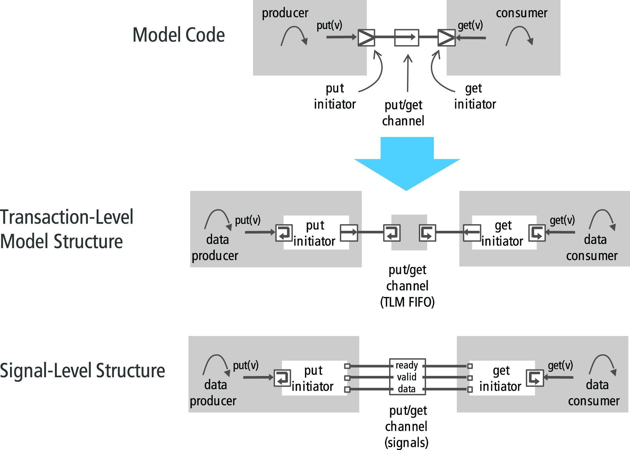
Diagram 1.0: Flex Channels
A highly productive software-driven SoC design flow, as shown in Diagram 2.0, relies on the design and verification progressing concurrently, from a high level of abstraction all the way to gate-level implementation. For verification, the focus is to verify functionality at the highest possible level of abstraction available, and then avoid duplication of effort by directing additional verification activities towards the new and modified design functionality added at each stage of the design refinement process.
The goal is a single common verification environment that spans the different abstraction levels of the SoC design. A single common verification plan is defined such that it outlines the features to be verified in each specific level of design. As architectural decisions are made that bring the design closer to implementation, the verification environment is concurrently extended to test those architectural choices.
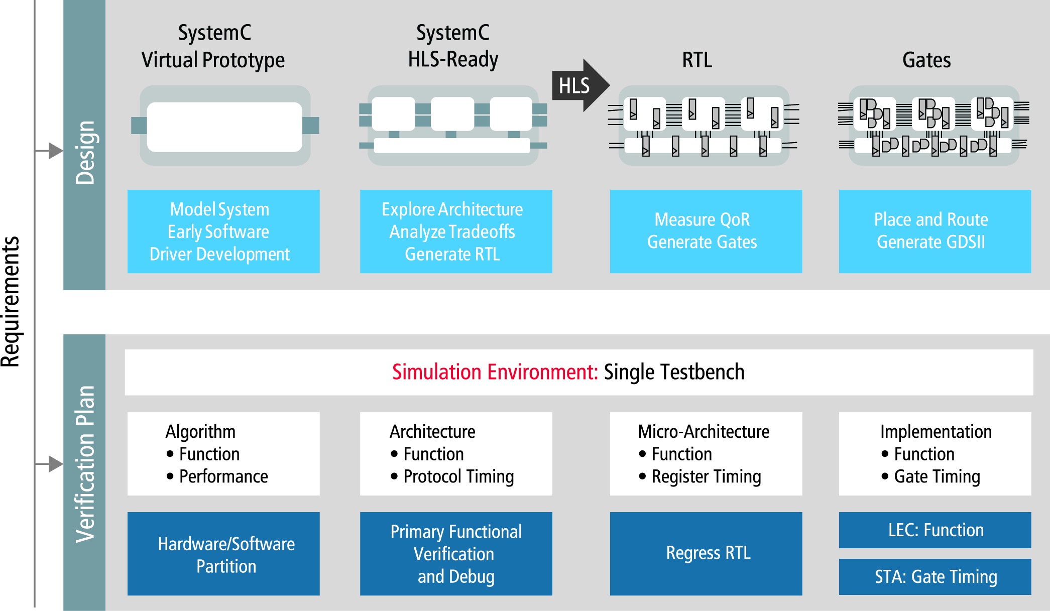
Diagram 2.0: TLM-Based Design Flow
Metric-Driven Verification Meets Metric-Driven Creation
Verification of TLM IP has many advantages over the verification of RTL IP. TLM verification is inherently fast due to the simpler elaboration of high-level code and the smaller number of simulation events. We are proposing a high-level SystemC golden model in which the TLM channel and signals coexist. However, we can still create designs that optimize power, area, or performance by making different micro-architectural choices. Since the SystemC TLM IP block design can be expressed in 80% fewer lines of code than RTL, this minimizes the number of potential bugs while promoting functional verification at the interface, function, and protocol levels. The positive productivity gains inherent in this level of code compaction are represented in Diagram 3.0.
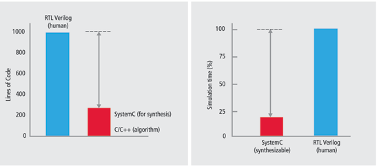
Diagram 3.0: Productivity gains with software-driven SoC design
There will be areas in which the TLM model will need to interface to RTL. This could be in a context where legacy IP exists in RTL form. In this context the TLM and RTL can exist in a hybrid simulation where custom-built transactors are used to interface the TLM and RTL together for simulation purposes.
A multi-level functional verification testbench is based on transactions. When the testbench is connected to RTL-based IP buses or interfaces, a transactor can be used to translate between the transaction-level domain and the pin-accurate RTL domain. The TLM verification methodology must consider how these transactors operate in order to gain the maximum advantage of a mixed TLM/RTL verification.
Acceleration hardware is seeing increased usage for system-level verification that includes one or more modules at the RTL level. Verification IP (VIP) must be equally applicable to these environments and must fully support metric-driven verification (MDV) techniques that allow coverage metrics to be maintained across the different levels of design abstraction. Transactors will need to serve as a bridge between software simulation, hardware acceleration, and testbenches.
MDV is an approach to the verification problem that begins after virtual prototyping and transforms an open-ended verification process into a repeatable, closed-loop process. Through this process, design and verification teams increase the quality of the SoC hardware in less time with fewer project resources. The four fundamental steps of MDV include plan, construct, execute, and measure-and-analyze.
The plan stage involves reviewing the functional specification of the design and determining what functionality must be verified at each development stage of the design IP. It is a goal of the verification plan to verify full functionality at the highest level of abstraction. Tests should be run post synthesis to ensure a total functional match between abstract model and implementation. As the verification plan is refined, it is not necessary to re-run all tests at these intermediate stages. Formal equivalence checking can be used where possible, or sequences can be re-used at subsequent stages to regress what has already been verified.
The construct stage involves deciding between the degree of formal or dynamic verification, where functional coverage or code coverage will be deployed, and whether directed test or constrained-random methods will be used for stimulus creation. Typically the verification environment for dynamic execution is constructed using the Universal Verification Methodology (UVM) framework. UVM is an industry-standard, open multi-language framework that enables reuse though modularity and ensures the verification environment can work together and operate at different level of abstraction. The execution stage extensively exercises the design using any number of available verification tools. This may involve both static and dynamic forms of verification.
The measure-and-analyze stage involves the automatic capture of metrics defined in the planning step to provide objective data with which to manage the verification project and to locate deficiencies in the plan or its execution. Notable metrics to capture and analyze include coverage analysis, failure analysis, charting and reporting, and closing off the process loop.
Metric-driven creation is an approach by which the constraints that will dictate the power, area, and performance of the HLS design are specified. The stages of metric-driven creation match up with the approach and timing of the MDV as shown in Diagram 4.0. In planning, the functional and algorithmic computational specification is reviewed for concurrency definition, memory structures, and clock domains.
In defining concurrency, we try to exploit the natural hierarchy of algorithms. The key to any algorithm is to map the concurrency of the algorithm and the control or sequential aspects of the algorithm. This helps us define the most efficient implementation in hardware. Synthesis will uncover low levels of concurrency, but higher levels of concurrency must be specified by the designer. High-level architectural planning has a significant impact on the types of solutions that can be explored during the HLS process. Clock domains are specified for all of the concurrent blocks.
In the construct stage, the architectural transformations that can affect area/timing, performance/latency, and power are all reviewed. This involves TLMs that are fully defined with TLM ports and flex channels and, therefore, allow an efficient mapping of signal-level interfaces directly into the RTL implementation. During this stage, a script is defined that provides a set of constraints that direct the actions of the HLS tool. The HLS tool will make all of the necessary changes to the micro-architecture, share resources, flatten arrays or utilize multi-port RAMs, and pipeline loops and functions while managing latency such that the design implementation results in a finished first-pass RTL design.
The execution phase involves the final architectural choice and constraints. The measurement and analysis section involves reviewing reports and graphical information on the results of the synthesis optimization. Critical paths can be further analyzed and graphical tree views of power and area can be used to identify areas for improvement. Pipeline implementation and the design control and dataflow graphs can also be reviewed. This allows us to close the design loop concurrently with closing the verification loop.
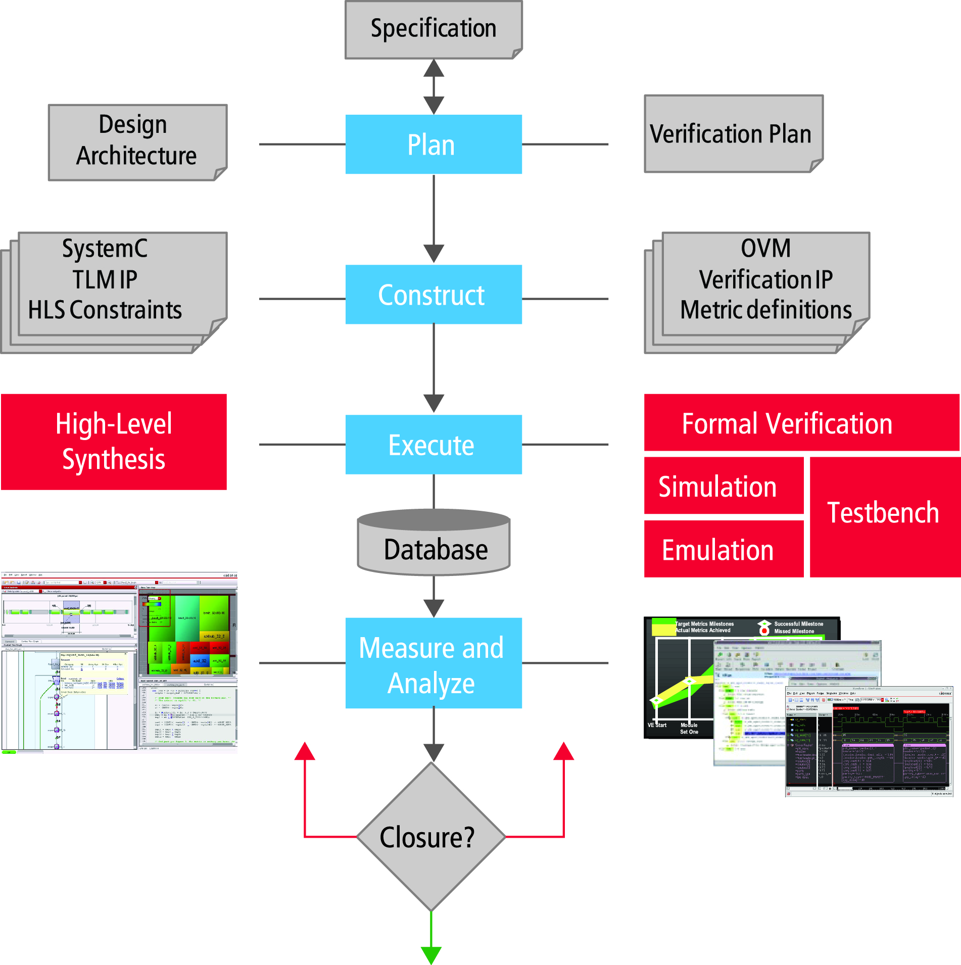
Diagram 4.0: Metric-driven verification and metric-driven creation
Putting MDV and MDC Into Practice—and Expanding the HLS Application Space
In using MDV and MDC together to drive productivity, the testbench must be configured at each verification level. While the rest of the code is reusable, the configuration tasks must be aligned with the specific level of abstraction. Some of the configuration tasks that require attention include: verification hierarchy, connecting the clock and reset signals, configuring the transaction-level verification component, connecting the TLM interfaces between the testbench and the model, and providing white-box monitoring for viewing embedded variables.
Applying MDV and MDC in combination requires an advanced HLS tool. Early HLS tools tended to focus on datapath-only style designs. Furthermore, many of the early HLS tools constrained the target of these datapath designs to FPGAs versus ASIC designs to minimize the level of optimization that was needed.
Today, there are SystemC-based HLS tools that can easily handle designs that are all datapath, all control, or a mixture of both types of design. Additionally, some HLS tools now directly include production logic synthesis tools. These new HLS tools can be applied to a much wider variety of applications that can directly benefit from software-driven SoC design and SystemC-based TLMs that span design and verification. Diagram 5.0 shows a number of new application areas in which customers are now applying HLS.
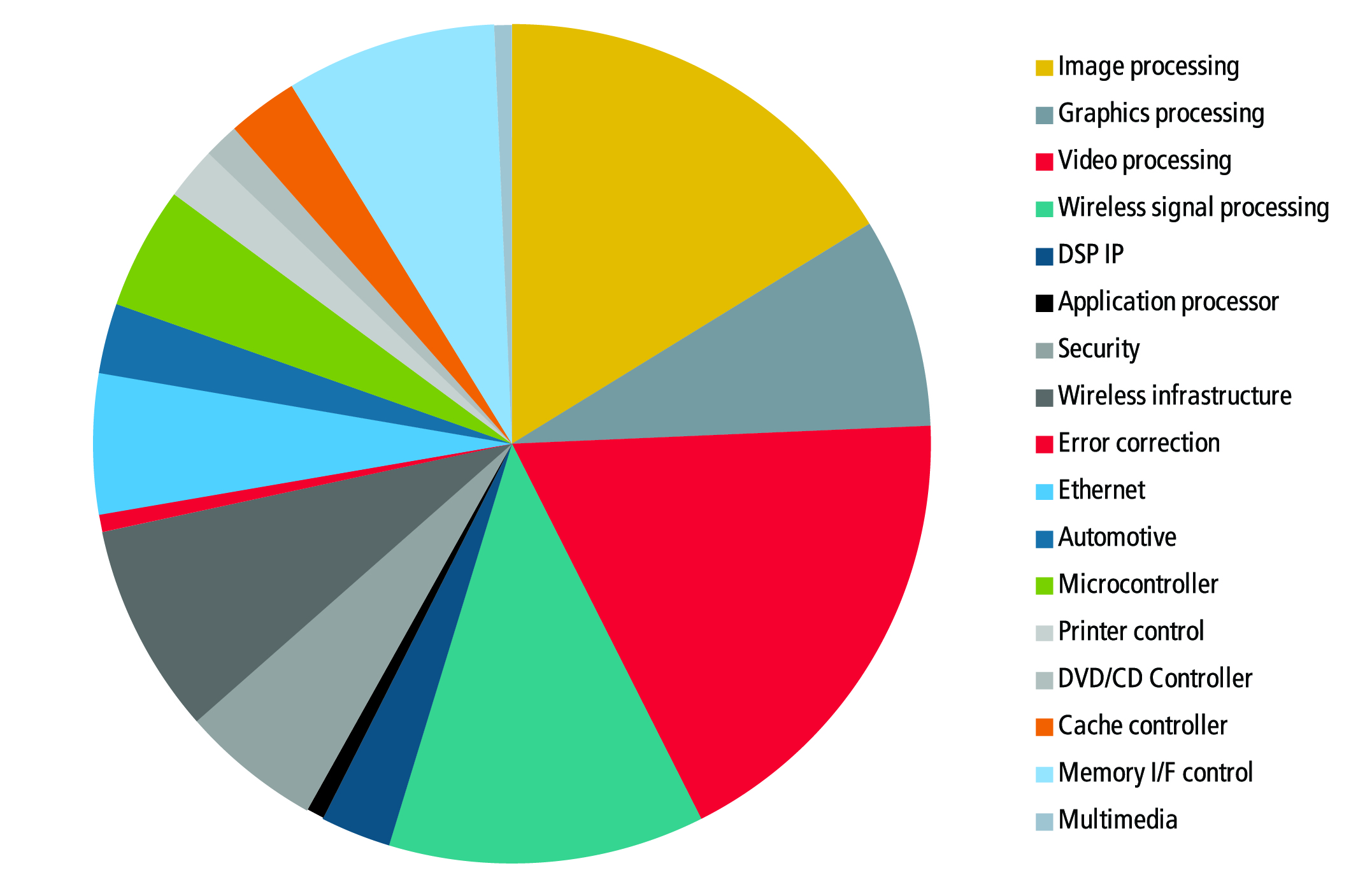
Diagram 5.0: The expanding application domain for HLS
Summary:
Software-driven SoC design flows are being enabled by the emergence of transferable SystemC TLM models for both virtual prototyping and HLS implementation. The opportunity to create a full-scale SoC design faster, with fewer resources and better results, is now upon us. By using a single unified TLM format for design and verification, metric-driven creation and MDV can be used to concurrently build and analyze an SoC design.
About the Author:
 Phil Bishop is the Vice President of R&D for System Level Design at Cadence Design Systems (San Jose, Calif.) ??Phil joined Cadence Design Systems in 2012 and has 30 years of experience in the Electronics Industry. Prior to joining Cadence, he was Corporate VP of Marketing for Magma, and before that he was the CEO of two startup companies in the EDA market, Pyxis Technologies and Celoxica Holdings. Phil also held leadership positions at Mentor Graphics, Motorola, and Boeing. Phil Holds an MBA from Duke University and has two engineering degrees from the University of Michigan.


Cadence’s Phil Bishop talks about leveraging TLM and SystemC for both design and verification. What do you think?