


Everyone is jumping on the 3D bandwagon. But if I said that MEMS was just taking some steps in that direction, you might understandably question my mental health, since, at first blush, it would seem that MEMS structures are already 3D.
After all, that most primitive MEMS element, the cantilever, to name one example, is specifically intended to move out of the wafer plane – why is that not 3D?
The movement of the cantilever may be 3D, but the structure is only quasi-3D, as explained in an MIT paper by Fabio Fachin, Brian Wardle, and Stefan Nikles. Deep reactive ion etching (DRIE) has been fundamental to MEMS on silicon, but, almost by definition, all it does is take a 2D image and project it deep into the silicon. A separate etch can then release the structure by etching underneath. But, for all of these typical MEMS elements, they represent a planar pattern printed with a mask that’s then given some depth. There are no curves or other features that are out of the wafer plane.
There are techniques using polymers that can create 3D elements, but some MEMS functions rely on a much higher Young’s modulus (which measures the “springiness” of a spring) than the relatively “mushy” polymers can provide, turning instead to springier materials like silicon.
There are also ways of achieving some out-of-plane characteristics via so-called “post-release” steps. Typical is to use a probe tip to push the end of a cantilever down and “snap” it into some anchoring structure at the bottom. But these techniques rely on such external forces to establish the configuration. What the MIT team was trying to do was to let the 3D nature establish itself by careful design of residual stresses that would shape the structure at the release step itself.
The “poster child” structure they illustrate is that of an arch. There are really two pieces to the question of how this can be done. First, are there techniques for causing a silicon beam to deform up or down into an arch when released? And second, can the details of the resulting configuration be predicted analytically up front so that you can design in exactly the amount of arch height desired?
The answer to both is, “Yes,” and, as you can imagine, much of what the team has published consists of the math that backs up their design technique. It involves analysis of the mean and gradient stresses as well as the effects of “clamping” – the fact that the ends of the beam are held in place and can’t move, which tosses in some non-idealities.
We won’t delve into the math. (You’re welcome.) But we will look at a number of mechanisms they have used to create and control the forces that cause the buckling that results in arch formation (either up or down).
Designers have limited flexibility in creating stress directly in silicon. The team was able to create a three-axis “thermal accelerometer,” however, through direct control of the silicon residual stresses. This IMU works on a completely different principle from the ones we’ve looked at before. Instead of relying on mechanical deflection, a heater is used to heat a “fluid” (possibly just air), and then sensors (thermopiles) are placed around the heater. At rest, the heat should diffuse outward evenly to the sensors; if the body is accelerated, that diffusion won’t be even, and the differential signals the acceleration. (Frankly, it astounds me that such a sensitive effect can be reliably detected.)
But if such a sensor is to allow detection in all three axes, then sensors must be placed out of the plane of the heater element. In their example, this is done by placing the heater on a straight in-plane beam and then putting the x-y sensors on the tops of arches placed on either side of the heater. The z sensors are built on “tethers” – essentially curved cantilevers – that are placed on the arches, raising the z sensors even higher than the x-y ones.
While this technique worked, they went further to come up with ways of giving designers more leverage (so to speak) in creating a wide variety of structures. They have identified three ways of achieving an arch from a beam: using “patches,” “step-ups,” and “runners.”
Patches are materials with engineered compressive or tensile stress that are placed at the ends of the beams, as shown in Figure 1. The patches are engineered either to push down or pull up on the beam at the point of overlap.
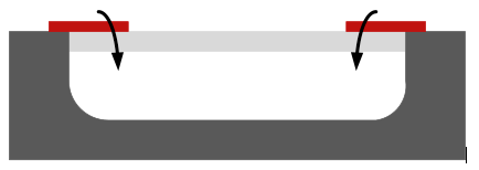
Figure 1. “Patch” configuration (edge view). As shown, the patches push down on the beam, although they could be used to pull up.
Step-ups, on the other hand, don’t lie over the beam; they abut the beam, as shown in Figure 2. The wall of the step-up that meets the beam is slightly off vertical. As shown, this pushes down on the beam; if the slope were in the other direction, it would arch the beam up by placing more stress at the base of the beam instead of the top.
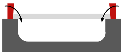
Figure 2. “Step-up” configuration (edge view). The non-vertical wall pushes on the top edge of the beam, forcing the beam down; the step-up slope could also go the other way to pull up on the beam.
Finally, runners are used only to guide the beam on release. A runner is a parallel beam with stress engineered in the desired direction. It’s connected to the beam by a number of “micro-bridges” (Figure 3; note that this is a top view, while the other two are edge views). The etch sequence is set so that the runner is released first, allowing it to take on its shape (arched either up or down). That then coerces the beam in the same direction when it’s subsequently released. The runner is then disconnected from the beam, possibly to be removed completely.

Figure 1. “Runner” configuration (top view). Stresses in the runner bias the shape of the beam.
They’ve built all of these structures, but what’s notable is not simply the fact that it’s possible to do this, but that they can engineer specifically what the stresses will be so that they can position the elements explicitly (rather than just bending a beam and living with whatever arch results).
This is still university research work, so it’s not clear when this will hit a theater near you, but it does feel like a significant step to be able to incorporate an extra degree of freedom in a design.
More info:
I usually don’t like to put links to papers that are blocked by paywalls since it’s mostly just frustrating. But it seems like I should provide a way to get to this paper. It will eventually be available for free on MIT’s website (since they have an open access policy), but they can’t do that until it’s been published elsewhere, which only just happened on IEEE. If I get the free link in the future, I’ll put it here. For now, here’s the current link to the issue that contains the article (pp 1-14). Given that the link has a “recentissue” component, this may not work forever…


What would you like to build if you had this extra degree of freedom?