


The number of wireless enabled systems is very diverse and steadily growing. System makers include wireless functions into mature applications like fixed-line telephones and TV’s, increase the wireless features in mobile phones with support of multiple standards and come up with new device types that thrive on being always wirelessly connected for the newest content [1]. Further, also the transport, security, medical and payment sectors are quickly switching to wireless interfaces for improved user experience. Intelligent wireless bus, subway and train tickets replace the paper versions. Expensive equipment or resources in general are traced back thanks to RFID tags. Sensor networks reduce the cost of medical care while they increase the reaction speed when needed. Near Field Communication ‘NFC’ bank cards replace the smartcard and magnetic strips now commonly used.
Wireless communication comes in many forms, each designed or optimized for a specific task and application and sometimes constrained by local legislations differences [2]. Moreover existing standards are typically upgraded a few years down the road to enable higher data throughput or to extend the range [3]. Wireless standards can be grouped or compared based on different parameters like center frequency, primary use, encoding protocol, degree of mobility or range for instance. A rather complete overview of industry standards and proprietary formats can be found online [4].
Despite the improved ESD awareness and control in assembly factories and the related push for a reduction of component level ESD performance [5, 6] IC’s still need adequate ESD protection. In many cases, traditional ESD protection devices used for low speed digital interfaces offered by foundries, IO library providers are not suited for the RF interfaces for a number of reasons:
- Capacitive loading shunts large part of the RF signal to Vdd/Vss lines due to high parasitic junction and metal capacitance of ESD clamps.
- Increased noise injected at the receiver due to series resistance used between primary and secondary ESD clamps
- DC leakage current degrades Q-factor and influences the size of the bias circuits
To reduce the cost of consumer electronics devices designers also try to combine different standards into a single silicon die [3] adding more constraints for the ESD protection approaches: the clamp parasitic influence should be as stable as possible across a large frequency band and voltage range.
I. ESD approaches for wireless interfaces
IC designers use a variety of ESD protection approaches to protect the integrated circuits against ESD stress. The well known ‘dual diode’ based ESD protection has been used by many designers for the protection of analog circuits thanks to the small area, straightforward implementation, low leakage and low capacitive loading. Recently however various researches have predicted the end of ‘dual diode based ESD design’ for RF circuits in advanced CMOS (65nm and beyond) due to the shrinking ESD design window of the sensitive circuits [8-13]. They reason that to ensure effective protection the diodes connected to the IO’s must be designed with larger perimeter to reduce the voltage drop (Ron x IESD) which in turn leads to higher leakage and higher capacitive loading worsening the RF performance of the connected circuits.
Fortunately there are alternatives to protect RF circuits against ESD stress. This section very briefly outlines different protection approaches [11, 14] and provides relevant references:
(1) Plug-n-play, minimal parasitic capacitive loading
The parasitic capacitance of the ESD devices is minimized such that the degradation of the RF performance is limited. Researchers have compared different device types for this purpose [15-17]. Besides the active ESD devices people have used low frequency filters for high frequency applications (>5GHz) [18-21]
(2) ‘LC’ Cancellation techniques
In various publications designers compensated the parasitic effects of ESD devices by adding tuned LC elements [10, 13, 22]
(3) Co-design
Through the use of ‘co-design’ traditional ESD solutions with high capacitive loading can still be used because the negative effects are compensated for in the matching circuits [23, 24].
The following sections provide case studies based on one specific protection approach: plug-n-play protection with low capacitive SCR based protection.
II. SCR based RF protection in 40nm LP
This section outlines various SCR based approaches for ESD protection of wireless interfaces in a 40nm Low Power CMOS technology. First the different device types and measurement setups are described followed by the measurement results. Finally the most appropriate ESD protection device is selected based on the TLP, HBM, RF/S-parameter and DC leakage measurements.
II.A. Device types
Two different SCR based protection clamps are compared for 1.1 V (1.2-V overdrive) RF interfaces. The variation between the clamps is mainly related to the trigger concept. Figure 1 provides an overview of the two clamp devices including a top view of the layout.
- The ESD-on-SCR is triggered as soon as the IO level raises 1 diode drop (Anode-G2) above the Vdd voltage [26].
- The diode-triggered silicon-controlled rectifier (DTSCR) is turned on once the Anode-G2 and 3 trigger diodes are forward biased [27, 28].
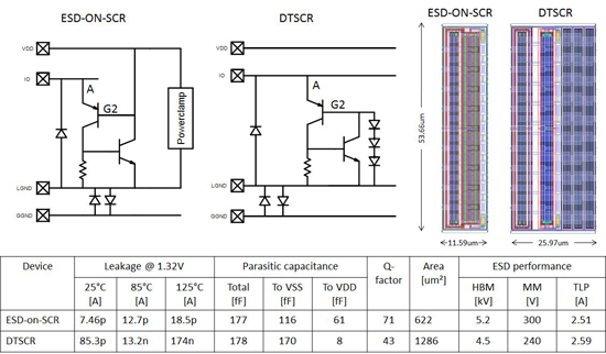
Figure 1: Overview of the 2 SCR based ESD clamps used in this work. The schematics are depicted on the top, left. The ESD-on-SCR is triggered as soon as the IO level raises 1 diode drop (Anode-G2) above the Vdd voltage. The DTSCR is turned on once the Anode-G2 and trigger diodes are forward biased. Layout comparison of the clamps is shown top, right: Due to the trigger diodes, the DTSCR clamp (1286um²) is twice the size as the ESD-on-SCR clamp (622um²). Measurement results are summarized in the table.
Besides these two main types some other variations were combined on an RF test chip to validate SCR based protection for low-noise amplifier (LNA) circuits.
All SCR clamps are designed for 2kV HBM and 200V MM which corresponds to more than 2A of TLP current in the TSMC 40nm process technology. The SCR perimeter of 2x47um is the same for all devices. All use 4 layers of metal leaving all other layers for bus routing. To limit noise coupling all devices described here use the deep Nwell layer.
Each clamp type is connected to an impedance-controlled Ground-Signal-Ground pad group to obtain accurate capacitance and Q-factor values. De-embedding structures (short, open), which allow the characteristics of the circuit to be isolated from those of the measurement fixtures, are available too (Figure 2).
ESD devices are available as stand-alone clamps (for accurate leakage tests) and with 2 different monitor structures, which act as test proxies for real circuits that need to be protected, to characterize the effectiveness of the ESD protection: (1) The ‘GOX’ monitor [25], which mimics circuits having a thin gate oxide, is a minimum size, fully silicided thin oxide transistor with gate connected to the IO pad. (2) The ‘RC-MOS’ monitor, which mimics circuits with an RC filter before the gate of an MOS transistor, is a minimum size, fully silicided thin oxide transistor where drain is connected to pad, source to ground and gate is biased at 1/3 of the drain voltage through an RC-filter scheme.
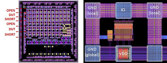
Figure 2: 40nm RF test chip overview (left) and GSG layout example for a single clamp cell (right). The S-parameters are de-embedded to the edge of the ESD-clamps. An individual OPEN and SHORT structure is provided for each clamp.
II.B. Measurement setups and results
The different SCR clamps and monitor structures are measured with Transmission Line Pulse (TLP), HBM, MM, DC leakage and S-parameter systems.
The TLP data is performed with a Barth Electronics (10ns rise time, 100ns pulse width). For all devices positive stress is applied to the IO pad while the local ground (LGND) is grounded. During TLP stress relay S1 is open (Figure 3) but in order to obtain accurate leakage current results the substrate needs to be grounded through the global ground pad (GGND) by closing relay S1 during the leakage test. For some devices, a diode is present from IO to VDD. This results in an additional leakage path through the diode from IO to VDD and through the power clamp to LGND/GGND. The leakage current for these configurations is still low enough to detect failure if the VDD pad is left floating. Therefore the VDD pad is not powered during the leakage test. The maximum current level ‘Imax’ is defined as It2 failure current minus a 20% safety margin.
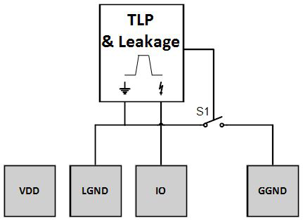
Figure 3: TLP measurement setup: During TLP pulsing between IO and ground the global ground ‘GGND’ is not connected. For leakage measurements in between ‘zaps’ the global ground (and complete substrate) is connected together with the local ground ‘LGND’. Vdd remains floating during the TLP/leakage tests.
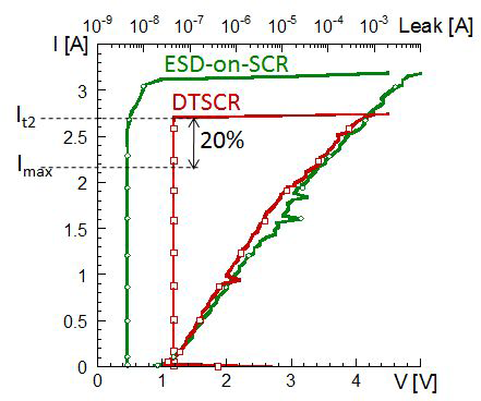
Figure 4: TLP IV curves for the 2 device types: The clamping behavior is identical.
Figure 4 and 5 plot the TLP IV curves of the 2 devices. The clamping device (SCR) is the same in the 2 device types also evident from the figures: the clamping behavior is exactly the same. The failure current It2 is more than 2.5A. After subtracting a safety margin of about 20% to cover process variations the maximum current level (‘Imax’) is more than 2A for all devices. As expected, the triggering of the ESD-on-SCR is strongly different compared to the DTSCR and makes it more effective for protection of sensitive circuits.
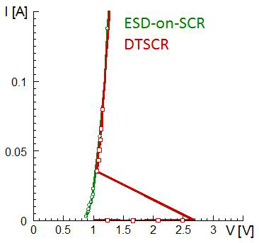
Figure 5: Zoom-in on the TLP IV curves for the 2 device types: The trigger voltage of the ESD-on-SCR is much lower than the DTSCR.
Besides standard TLP tests each clamp is also stressed with multiple pulses according to the same test setup. At least 1000 TLP pulses are applied with current amplitude fixed to the maximum current level ‘Imax’ [25, 29]. The leakage current is measured after each set of 100 pulses. Failure is defined as any significant or systematic deviation from the pre-stress leakage current. All devices passed this test condition without leakage increase.
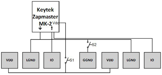
Figure 6: Measurement setup for HBM/MM measurements. VDD and GGND are only connected during the curve trace phase by closing switch S1 and S2
HBM, MM measurements are applied to the IO pin with all LGND pins grounded and with VDD and GGND floating. The DC sweep between zaps is performed while both GND and LGND pads are grounded and 1.32V bias is applied to the VDD pad. Figure 6 illustrates the measurement setup used for the HBM and MM tests. Minimum pass level for HBM and MM measurements is given in the table in figure 1, based on data of 6 samples (3 with ‘GOX’ monitor and 3 with ‘RC-MOS’ monitor).
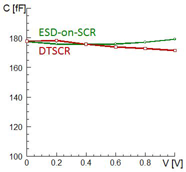
Figure 7: S-parameter analysis at 5GHz- average of 4 dies. Influence of the total IO capacitance versus IO voltage: Both devices show a rather small variation in parasitic capacitance.
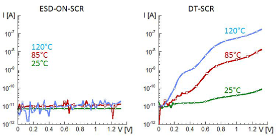
Figure 8: Comparison of the DC leakage measurements at three temperatures (25°C, 85°C and 120°C) between the two SCR types in this study. To measure the clamp related leakage individually all test structures were measured without monitor devices. The basic SCR in 40nm has an extremely low leakage (~10pA) that is very stable across temperature. This is visible in the leakage measurements on the ESD-on-SCR device (Vdd is biased at 1.2V). The leakage current for DTSCR is determined by the trigger element. The leakage difference can be used to select the lamp with the highest Q-factor: The ESD-on-SCR has the lowest leakage and the highest Q-factor.
During DC leakage measurements both global and local ground pads are connected and grounded. The supply pad (VDD) is biased at 1.32V DC. The voltage at the IO pad is swept linearly from 0V to 1.32V. The measurements are performed on devices without a monitor device to accurately measure the clamp leakage. The measurements are performed on die, in the dark and at three temperatures: room temperature (25°C), 85°C and 120°C. Figure 8 summarizes the data for the two device types.The measurements on the ESD-on-SCR show that the intrinsic leakage of the SCR device is very low even in 40nm CMOS (~10pA). The leakage of the DTSCR is determined by the trigger element: the leakage stays below 100pA when a diode chain is used to trigger the SCR. The leakage current has a strong relation to the Q-factor of the ESD clamps: The table in figure 1 shows that the Q-factor of the ESD-on-SCR (lowest leakage) is 1.5 times higher than that of the DTSCR where the leakage is 10 times higher.
Finally, the different clamps were measured with RF S-parameter equipment. After de-embedding based on ‘open’ and ‘short’ structures, the device parasitic capacitance (junction and metal combined) is determined as a function of IO bias voltage (between 0 and 1V) and frequency (between 1 and 20 GHz). Both plots (Figures 7 and 9) show that the capacitance level variation is less than 6%.
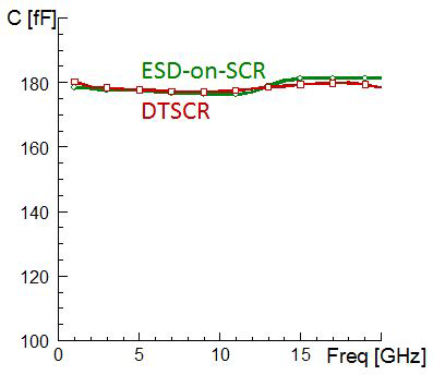
Figure 9: S-parameter analysis at 0V IO bias, average of 4 dies: Influence of the total IO capacitance versus signal frequency: Both device types have a small variation in capacitance value.
Besides the standard devices described above additional variations are included on the test chip including capacitance reduction circuits, SCR anode/cathode layout variations and versions without deep Nwell. A summary of the ESD, Q-factor and capacitance values is given in figure 10.
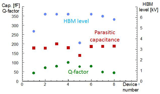
Figure 10: Various layout variations were available on the RF test chip. High ESD performance combined with low leakage, high Q-factor and low parasitic capacitance loading can be easily achieved in 40nm.
II.C. Selection of the most appropriate ESD clamp
Based on the different measurements the recommended protection solution for LNA circuits in 40nm is the ESD-on-SCR. While the parasitic capacitance is similar between DTSCR and ESD-on-SCR devices, the latter has much lower leakage current, higher Q-factor and a much smaller silicon footprint. The ESD data shows that the ESD-on-SCR provides an effective protection of more than 300V MM and 5.2kV HBM. However, in many cases the required protection level is only 2kV HBM. Thanks to the simple layout style and straightforward metallization concept the ESD-on-SCR can be easily scaled down to lower the ESD performance leading to further reduced leakage (below 10pA), capacitance (~100fF) and silicon area (~500um²).
Important to note is that the ESD-on-SCR is triggered into low voltage clamping mode as soon as the IO voltage raises 0.7V above the Vdd potential (1.2V). For the LNA circuits described here this is not a concern: The applied signal has no DC component. Also, the bias circuit has a high output resistance and the bias level is somewhere between 0.3V and 0.5V much lower than the SCR holding voltage. Moreover, the input signal from the antenna has a low amplitude which means that the trigger condition for the ESD-on-SCR is never fulfilled. For the protection of other applications in advanced CMOS the SCR can easily be tweaked to solve most latch-up constraints including transient latch-up situations during system level stress [30, 31].
If the Vdd line is rather noisy it could couple to the RF IO pad. Therefore, some designers may prefer the DTSCR device type because it has much less parasitic capacitance between IO and Vdd.
Conclusion
This publication provided information about SCR based ESD protection clamps for RF circuits validated in TSMC 40nm LP CMOS technology. The ESD protection clamps described have excellent figures of merit: Due to the low parasitic capacitance, low leakage and high Q-factor the influence on the RF performance is limited. RF designers can rely on these SCR device types without the need for extensive co-design optimizations between RF (matching) circuitry and ESD protection devices.
The paper provided measurement results on TSMC 40nm RF LNA’s where the sensitive thin oxide circuit is effectively protected up to 5.2kV HBM while the leakage stays below 10pA and the parasitic capacitance is around 180fF over a broad range of frequency and voltage.
While this paper focused on Bluetooth, GPS the ESD device concepts can be used more broadly for both high frequency RF IO’s as well as high speed differential, digital interfaces like HDMI and USB 3.0.
Note
As is the case with many published ESD design solutions, the techniques and protection solutions described in this paper are covered under patents and cannot be copied freely.
References
[1] ITU Internet Reports 2005: The internet of things
[2] http://www.newscientist.com/blogs/shortsharpscience/spectrum.png
[3] F. Louagie, “Building tomorrow’s wireless communication systems”, 2009
[4] http://en.wikipedia.org/wiki/Comparison_of_wireless_data_standards
[5] White Paper, “A case for lowering component level HBM/MM ESD specification and requirements”, 2007 http://www.esdforum.de/
[6] White Paper, “Recommended ESD-CDM Target Levels”, 2009, JEP157. http://www.jedec.org/standards-documents/results/JEP157ESD council
[7] http://en.wikipedia.org/wiki/IEEE_802.15.4a
[8] G. Boselli, “Analysis of ESD Protection Components in 65nm CMOS: Scaling Perspective and
Impact on ESD Design Window”, EOS/ESD 2005
[9] J. Borremans et al., “A 5 kV HBM transformer-based ESD protected 5-6 GHz LNA”, VLSI 2007
[10] S. Hyvonen, et al., “Comprehensive ESD protection for RF inputs,” EOS/ESD 2003
[11] S. Thijs et al., “Implementation of plug-and-play ESD protection in 5.5 GHz 90 nm RF CMOS LNAs—Concepts, constraints and solutions”, Microelectronics Reliability 2006
[12] Ph. Jansen et al., “RF ESD Protection strategies – The design and performance trade-off challenges”, CICC 2005
[13] S. Joshi et al., “High-Q Electrostatic Discharge (ESD) protection Devices for Use at Radio Frequency (RF) and Broad-band I/O pins”, IEEE transactions on Electron Devices 2005
[14] D. Linten et al., “ESD protection of Advanced RF and Broadband integrated circuits and MEMS”, IEW 2010
[15] Richier et al., ”Investigation on different ESD protection strategies devoted to 3.3 V RF applications in a 0.18 CMOS process”, EOS/ESD 2000
[16] M.K. Radhakrishnan et al., “ESD Reliability Issues in RF CMOS Circuits”, 2001
[17] Feng K et al. “A comparison study of ESD protection for RFICs: performance versus parasitic”, 2000 IEEE RFIC
[18] S. Thijs, et al., “Implementation of Plug-and-Play ESD Protection in 5.5 GHz 90 nm RF CMOS LNAs – Concepts, Constraints and Solutions,” EOS/ESD 2004
[19] S. Thijs et al., ”Inductor-Based ESD Protection under CDM-like ESD Stress Conditions for RF Applications”, CICC 2008
[20] D. Linten et al., “A 5-GHz Fully Integrated ESD-Protected Low-Noise Amplifier in 90-nm RF CMOS”, JSSC 2005
[21] S. Thijs et al., “CDM and HBM Analysis of ESD Protected 60 GHz Power Amplifier in 45 nm Low-Power Digital CMOS”, EOS/ESD 2009
[22] S.Hyvonen et al., “Cancellation technique to provide ESD protection for multi-GHz RF inputs”, EL 2003
[23] W. Soldner et al., “RF ESD Protection Strategies: Codesign vs. low-C Protection”, EOS/ESD 2005
[24] V. Vassilev et al., “Co-Design Methodology to Provide High ESD Protection Levels in the Advanced RF Circuits”, EOS/ESD 2003
[25] C. Russ et al., “GGSCRs: GGNMOS Triggered Silicon Controlled Rectifiers for ESD Protection in Deep Sub-Micron CMOS Processes”, EOS/ESD 2001
[26] B. Keppens et al., “ESD Protection Solutions for High Voltage Technologies”, EOS/ESD 2004
[27] M. Mergens et al., “Advanced SCR ESD Protection Circuits for CMOS / SOI Nanotechnologies”, CICC 2005
[28] M. Mergens et al., “Diode-Triggered SCR (DTSCR) for RF-ESD Protection of BiCMOS SiGe HBTs and CMOS Ultra-Thin Gate Oxides”, IEDM 2003
[29] B. Keppens et al., “Contributions to standardization of transmission line pulse testing methodology”, EOS/ESD 2001
[30] Y. Fukuda et al., “Solving the problems with traditional Silicon Controlled Rectifier (SCR) approaches for ESD”, RCJ 2008
[31] B. Sorgeloos et al., “On-Chip ESD Protection with Improved High Holding Current SCR (HHISCR) Achieving IEC 8kV Contact System Level” IEW 2010 and EOS/ESD 2010
Authors:
B. Keppens, I. Backers, J. Binnemans*, B. Sorgeloos, O. Marichal, K. Verhaege
Sofics BVBA, Groendreef 31, B-9880 Aalter, Belgium – bkeppens@sofics.com
*now with ICSense – copyright 2012, Sofics
Image: Fir0002/Flagstaffotos


9 thoughts on “SCR based on-chip ESD protection for LNA’s in 40nm CMOS”