

What’s the difference between a FinFET and a FD-SOI transistor?
90°.
Admittedly, that’s the abridged version. And it would be met by howls of protest by the proponents of FinFETs and of FD-SOI transistors. Along with that right-angle rotation comes a ton of technology, accompanied by the skirmishing that comes with vested interests and big unknowns.
The stakes have been ratcheted way up this week with Intel’s blockbuster announcement of imminent FinFET – er – Tri-gate production – while the other FinFET proponents have been calmly trundling along, aiming at the teens of nanometers for FinFET use.
So what the heck is going on here? This exotic technology went from lurking in the weeds to exploding out onto the fairway. Well… let’s back up a second and take things one step at a time.
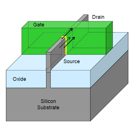
Let’s say we want to make a very fast, very small transistor. And we want to control the on/off current characteristics very carefully. This means we have to control the channel dimension more precisely than is possible by simply doping bulk silicon (OK, we can dope it, but it’s really hard – something easier would be better).
One way is to lay a thin silicon channel over an insulating material. Now you’ve got relatively strict dimensional control over the thickness – it’s got a hard stop underneath. You put gate oxide over the top and then deposit a gate electrode and, assuming you’ve also thought to provision a source and drain, you’ve got yourself a tiny transistor.
To be specific, you’ve got a fully-depleted silicon-on-insulator – FD-SOI – transistor. Fully depleted because the channel is thin enough to allow the field to deplete the entire channel (as opposed to partially-depleted, where the channel is thicker, and not depleted at the deepest points).
SOI technology has been around for a long time in its partially-depleted incarnation, but it has been relegated to specialized use because the base wafer is so much more expensive than sand – er – silicon. In the scenario just described, some might have an additional concern: with the silicon film as thin as it has to be – several atomic layers only – it becomes very hard to deposit that layer uniformly.
To address that, you might consider turning the whole thing 90° (conceptually, mind you) so that, instead of the sandwich lying flat, it’s lying on edge, looking like a fin. Now the channel runs vertically.
Kind of like one of those action movies where the car has to get through a really narrow slot and somehow manages to get up onto its side to slither through. Except this actually has to work in real life.
What you have then is a FinFET, named for obvious reasons. Also called a 3-D device (not to be confused with 3-D ICs, where dice are stacked using TSVs).
Not your average transistor
There are some subtleties to the FinFET that result in its having different names for slightly different configurations.
With a standard planar transistor, the gate oxide covers the channel on one side only: the top side. But when flipped into a FinFET, that top side is now, say, the right side. What was the bottom side, which was inaccessible, is now the left side. And it is now accessible. So you can run gate oxide completely over the fin: now the gate isn’t just on one side, it’s “surrounding” the fin on three sides, left, top (just a thin edge), and right.
Configured like this, with gate oxide (and a gate electrode) on all three sides, you have what Intel calls a tri-gate transistor. Which is slightly different from the type of FinFET where the oxide over the top edge isn’t gate oxide, but rather field oxide, so it doesn’t act as a gate. In that case, the gate is active only on the left and right sides, not the top, so it’s not a tri-gate.
Because both of these configurations have multiple gates (from the standpoint of a device designer), you also encounter the name MuGFET. The “multiple” description is a bit misleading, however: it really refers only to the fact that what is typically a single gate electrode happens to act on multiple surfaces. In most cases, it’s still only one gate from a circuit designer’s perspective. The term MuGFET seems to apply more generically to any transistor having this multi-surface nature (of which the FinFET is best known).
However, imagine that the gate electrode doesn’t surround the fin. Instead, let’s say it just approaches from the left side and affects only the left side, like an ocean wave that splashed up against the fin – and then froze right there. Well, now you can do the same thing with a separate electrode from the right side – it’s like the original, except that there’s no metal across the top to bridge the left and right sides. Now you have two independent gates. (Kind of…)
Usually the two gates are referred to not as left and right, but as the front gate and the back gate. (Another 90° mental rotation. Which makes no functional difference. Well… actually… that’s not true… but I’m getting ahead of myself.)
But we have to be a little careful here when talking about multiple independent gates. Just like with a planar transistor, a FinFET can have several gates in series, so that the channel doesn’t conduct unless all gates are on. But the front/back gate concept is different. Rather than two gates affecting two different parts of the channel, now you have two gates affecting the same part of the channel. A typical way of using this is to have one of the gates (typically the front one) act as the on/off switch, while biasing the other gate to adjust the VT.
You can also use multiple fins in parallel to increase drive strength, and you can configure devices with multiple sources and drains. All of which can result in devices looking more like a waffle than a transistor.
Just remember that, for a circuit designer (not a transistor designer), a tri-gate is one gate, and a two-gate transistor has more gates than a tri-gate. Yeah, confusing.
FD-SOI vs. FinFET
Of course, FD-SOI is still an option, if this all sounds a bit overwhelming. In fact, it’s almost as if, in the rush to these cool, sexy, finned creatures, the SOI guys are back there shouting, “Yo, wait, don’t forget about us!”
So, first of all, is it an either/or choice? Not necessarily. Horacio Mendez, who runs the SOI Consortium, sees FinFETs as likely dominating where the highest performance is needed. He sees FD-SOI as much more of a contender for mobile applications, acting like a “G” or “LP” technology version.
He also sees – or saw – FD-SOI as being in play at the 20-nm node, with FinFETS at the 14-nm node. And he’s not the only one with such a view – TSMC’s Sr. VP for R&D, Shang-Yi Chiang, in a discussion at TSMC’s annual technology symposium last month, also looked for FinFETs in the below-20-nm space, saying that TSMC can make devices, but they aren’t ready for complete circuits yet. Clearly this all changes with Intel’s readiness to use FinFETs more or less now (shipping in the second half of this year) at the 22-nm node.
So there are a couple things we need to address here. First, what are the tradeoffs between FD-SOI and FinFETs? Second, since FinFETs are so different, do circuit designers need to treat them differently?
Let’s start with the SOI question. Historically, the main issue with SOI has been cost. And, while that cost isn’t going down, the cost of silicon is going up: FinFETs are complex to process. The fin is etched out of bulk silicon – that’s a larger feature than would typically be created, except perhaps in the MEMS world – and MEMS devices are about 50 times bigger than a FinFET and not nearly as precise. So, once the fin is established, laying the source and drain can be very involved, potentially requiring selective epitaxial growth of new crystalline silicon.
The bottom line is that FinFETs are expensive to make, even if the base wafer is cheaper than an SOI base wafer. The jury is actually still out on which one will end up having lower overall cost, although Intel claims that FD-SOI adds about 10% to the cost, while their Tri-gate technology only adds 2-3%.
According to Mr. Chiang, you can do more strain engineering on FinFETs than you can on FD-SOI devices – this was a major decision factor in TSMC’s choice of the FinFET as their main thrust.
Strain involves improving electron and/or hole mobility by adding stresses to the silicon lattice. Forcing the lattice slightly more open improves electron mobility, since they have more space to move in; compressing it slightly helps hole mobility, since it sort of spits the holes out faster, like you might a watermelon seed.
In fact, Mr. Mendez said that FD-SOI currently uses no stress layers, and that, while strain engineering could be added, initial deployments would go as is.
The other advantage for FD-SOI, for anyone except Intel, is that it will be available sooner than FinFETs.
New considerations for FinFETs
Given that some will choose FinFETs, what might circuit designers have to do differently? Is this simply another transistor, with all the fancy 3-D-ness abstractable away?
For the most part, yes, assuming you’re using the transistor with one gate connection. It’s just a transistor. With a couple caveats.
The most surprising change is the fact that orientation now matters. When you implement a planar transistor, it doesn’t matter which direction it faces: you’re always interfacing with the top plane of the silicon, and so you are always dealing with the same crystal face. When you use the side, however, now it depends on which direction the transistor is facing. Different directions will expose different crystal faces, with correspondingly different behavior.
This can be useful: there’s a direction that will improve PMOS performance without altering NMOS behavior. That allows you to balance better the P and N devices.
The use of strain in the tightly-packed circuits that FinFETs allow may also add some complexity. Ric Borges, Sr. Product Marketing Manager for Synopsys’s Silicon Engineering Group (i.e., TCAD), said that, based on what they’ve seen on very compact circuits like SRAM cells, the range of influence of the stresses in a transistor is no longer limited to that one transistor: the cluster of transistors will all affect each other. So the compact models may have to be changed to reflect this, and simulations will need to take proximity into account.
Finally, there’s a major consideration that will affect any kind of transistor at this density, and it’s nothing new: it’s the continuation and intensification of that old bugaboo, variation.
First of all, we think of the introduction of dopants as essentially spraying (loosely speaking) a uniform cloud of material that gets uniformly deposited. But that’s not the case. Just as the universe is lumpy, so is the dopant distribution. We’re talking on the order of a dozen or so dopant atoms in each transistor, so different transistors will have different numbers, and they will therefore behave noticeably differently.
The oxide/silicon interface is another critical area. We’d like to think of the oxide conforming perfectly to the silicon surface, but, again, that’s not the case. Voids and imperfections affect device behavior and will contribute to variation between transistors.
So the race is on. The current odds have Intel first with their tri-gate FinFETs, followed by FD-SOIC, followed by FinFETs-for-the-commoner. But, given the recent goading by Intel, who knows how those schedules will play out?
And, once all is said and done, will FD-SOIC and FinFETs satisfy different mainstream needs? Or will one of them be relegated to specialty niches? It’s simply too early to tell.
Having a major high-volume producer cranking out billions of FinFETs per chip will definitely give that technology an edge. Whether or not that edge gets shared with the others remains to be seen.
(Image courtesy of Intel Corp.)


9 thoughts on “Kissing or Cussing Cousins?”