

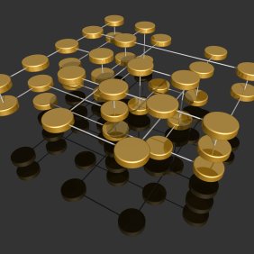
It’s all about degrees of freedom. The more of them you have, the more options you have. In the mechanical world, we think of it primarily as the number of dimensions within which you can move: a universal joint can bend in any direction because it has three axes of rotation, one for each of the three spatial dimensions. Three degrees of freedom. When an ant walks on a beach ball, even though it’s a 3-D object, it has only two degrees of freedom because it’s constrained to the surface of the ball. When routing signals on an IC, each layer provides additional degrees of freedom in two dimensions, with vias providing a third dimension that gets you from layer to layer.
Having more options can be good, but it also adds complexity. As any parent will know, just try giving a young boy full choice of what to wear to school: you’ll never get a decision. Restrict the decision to one of two shirts, and he can pick one and be on his way. Even scarier is the lockup that can occur if you offer a committee too many choices. Heck, give me a list of the dozens of possible cell phones and calling plans from which to choose, and I’m likely to end up quivering in a primordial cave, wishing the modern world would just go away and leave me alone.
So the benefits of choice are tempered by the stress of making life more complicated. From an IC perspective, adding degrees of freedom by using vias to interconnect metal layers on a chip is, of course, old news, and its complexities can be managed with well-established tools. It’s been taken a step further in the attempt to stack dice on top of each other using through-silicon via (TSV) technology. This provides an electrically clean, dense way of connecting signals from one chip to another by etching a hole through the silicon and filling it with metal. The earliest uses of this have simply stacked identical dice on top of each other for such purposes as increasing the amount of memory within a single package.
Such a die stack can use the cheap-and-dirtier “via-last” process for creating the TSV connections by having the assembly house make them with relatively coarse dimensions after the die has been made but before it’s been assembled. Much of this work can be done before the wafer is cut up.
But things get more interesting when you start to stack unlike dice. This kind of arrangement might be able to combine, for example, a processor with memory. In fact, perhaps two kinds of memory: volatile and non-volatile. You could throw an FPGA in there to boot. But here the dice are all different, so you can’t count on simply aligning the sides of identical dice; you now have a placement problem to figure out where things will go and what will stack on top of what. You might be able to fit two smaller dice next to each other on top of a larger die. You might want to stack things “tower of Hanoi” style to ensure that smaller dice always go on larger dice. Or, depending on the glue technology used, you might even be able to stack larger dice over small, allowing overlap. Oooo… here’s a cool one to think about: two small dice on a large die, and then a third die over the two small ones that bridges the two small ones, with some vias coming down on each die. I can already see some packaging engineers’ blood pressure rising.
If you’re going to create dice specifically for this, you can actually cut the die size down, while potentially improving performance. Knowing that you won’t be connecting to the outside world allows you to reduce the amount of routing on the chip, since you don’t necessarily need to go to the periphery. You can further shrink things by leaving off I/O-related circuits like ESD protection and clock recovery, since the signal won’t be traveling to the outside world.
When deciding where to put things, you could simply dedicate pads on a bottom die located exactly where the TSVs will come through on the top die. But you can get more degrees of freedom by creating metal layers on the bottom of the top die to redirect the TSV pads to some other location. These layers on the bottom of the die now act like the “interposers” inserted between a die and its package so that signals can be rearranged in a different order than they are on the die.
Of course, this now mandates the “via-first” process for adding the TSVs. Typically this means that, before the metal layers are added on top of the die, the TSVs are etched and stop somewhere down deep in the wafer, creating what is, for the moment, a blind via. The metal layers are then added on top and processing continues as normal. Once the topside of the wafer has been finished, the backside is lapped to thin the wafer down, eventually exposing the bottom of the TSVs. (Don’t we all wish we could thin our backsides that easily…) And now the two new metal layers can be applied to the backside, connecting to the newly accessible TSVs.
This adds degrees of freedom, which gives you more options. You now have lots of ways to arrange and interconnect stacked dice. So many that, in a conversation with Javelin’s Diana Raggett and Qualcomm’s Riko Radojcic, Riko’s standard answer to my numerous “Can you do ?” questions was, “It depends.” The number of options – and figuring out the impact of each one – have become complicated enough to warrant a tool from Javelin, developed in collaboration with IMEC, to help with what they call “pathfinding” – that is, figuring out the best 3-D arrangement.
Routing tools are obviously not a new thing in the chip world, but this is a bit different – it’s not the standard planar routing on metal layers (with interconnecting vias); it takes into account the metal layers on multiple chips (top and bottom), via placement, and chip positioning. It addresses the entire 3-D architecture, helping to evaluate the options.
The focus is on optimizing the electrical performance of the signals. While you would think that dealing with vias should be pretty straightforward, you’re not immune to the scourge of parasitics. Each via consists of a concentric oxide layer, within which the metal for the via is deposited. The oxide separates the metal from the bulk silicon, ensuring that you don’t get a surprise connection there. (Talk about yer sneak path…) But you still have a capacitor between the via metal and the bulk silicon, so its effects must be understood. Strictly speaking, you also have inductance, because, well, inductance is simply everywhere. But this isn’t a full package or board routing system, so it doesn’t actually handle inductance. While inductance could theoretically become a problem if frequencies got even higher, the fact is that frequencies aren’t going up on chips, so this solution is likely to remain adequate.
The one critical item that can’t yet be handled in the system is the effect of temperature. Thermal considerations become extremely important when stacking dice, because there is much more heat being generated within the package, and extra effort is required to sink the heat from the back of each chip – in fact, thermal spreaders sometimes have to be inserted between the chips.
While the routing considerations of any spreader can be handled in a pure routing tool, the Javelin system cannot yet help to figure out when and where cooling help is needed or whether the cooling solutions are sufficient. Once solid guidelines on how to do this are established, they can be integrated into the tool. For now, mechanical/thermal simulations are handled separately, although the results of the Javelin tool can be used as an input to such a simulator.
That leaves the real focus of the tool, for now, on managing the topological options: on helping to narrow down the choices, on taming the explosion of possibilities brought on by so many degrees of freedom. If it all works out, the problem becomes tractable. And if we’re really lucky, it will someday be able to return us to the innocence of our youth, offering us a blue shirt with racecars on it or a white shirt with green frogs on it, and all we’ll have to do is pick the one we want.


