


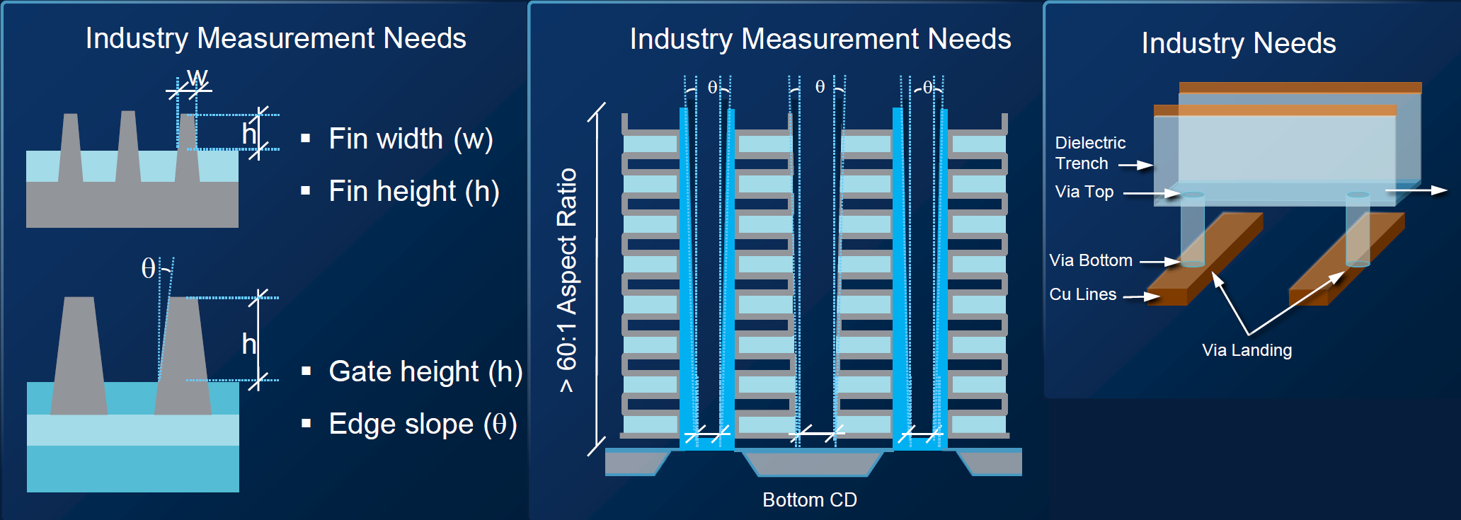
The 3D nature of aggressive silicon nodes continues to make life difficult for semiconductor equipment guys. Metrology is particularly troublesome, since seeing where edges lie isn’t always sufficient. I’m being somewhat liberal with the term “3D” since it involves more than just the usual 3D structures – FinFETs and 3D NAND stacks. I’m including the impact of multiple-patterning, which involves multiple overlay confirmations on stacks of masks that, in an earlier era, would have been a single mask. So they’re like a 3D decomposition of an erstwhile planar mask.
Let’s break the issues down. First is the fact that we’ve got new 3D dimensions to verify, and it’s hard to do with the old tools. As Applied Materials (AMAT) sees it, three specific structures are difficult: the two mentioned above (FinFETS, 3D NAND) plus vias placed at the bottoms of trenches for dual-damascene processes.
(Original images courtesy Applied Materials)
The issues are similar for the three structures, with variations:
- FinFET fins are sloped, and the angle matters. But it’s a slight angle, so it’s hard to see accurately with conventional approaches. If tight control can’t be achieved through metrology, then higher-power design techniques must be used to compensate for the variation.
- 3D NAND stacks have a similar, although inverted, challenge. After all of the films have been layered, holes are drilled all the way through. Problem is, they’re not really drilled; they’re etched, and they also have a slight taper to the edge that must be measured. And it’s extremely difficult to see the bottoms of the holes, since SEM electrons that go into the hole mostly don’t come back out. More on that in a minute.
- The in-trench vias start at the bottom of the trench and go down from there. It’s very hard to confirm whether, for instance, the bottom of the via has been suitably cleared out so that the via metal can make a good contact with the underlying metal line.
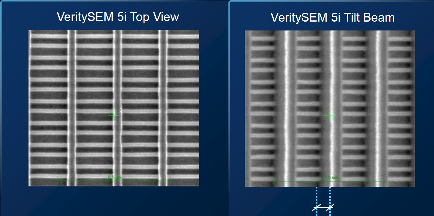
AMAT has done a couple of things to address these. For the FinFET issue, it’s applied a surprisingly simple solution: tilt the angle of incident light when measuring. They use 5° and 15°, and you can see the difference between straight-on light and tilted light in the following images. The tilted-light image illuminates the slope enough to make measurements.
(Image courtesy Applied Materials)
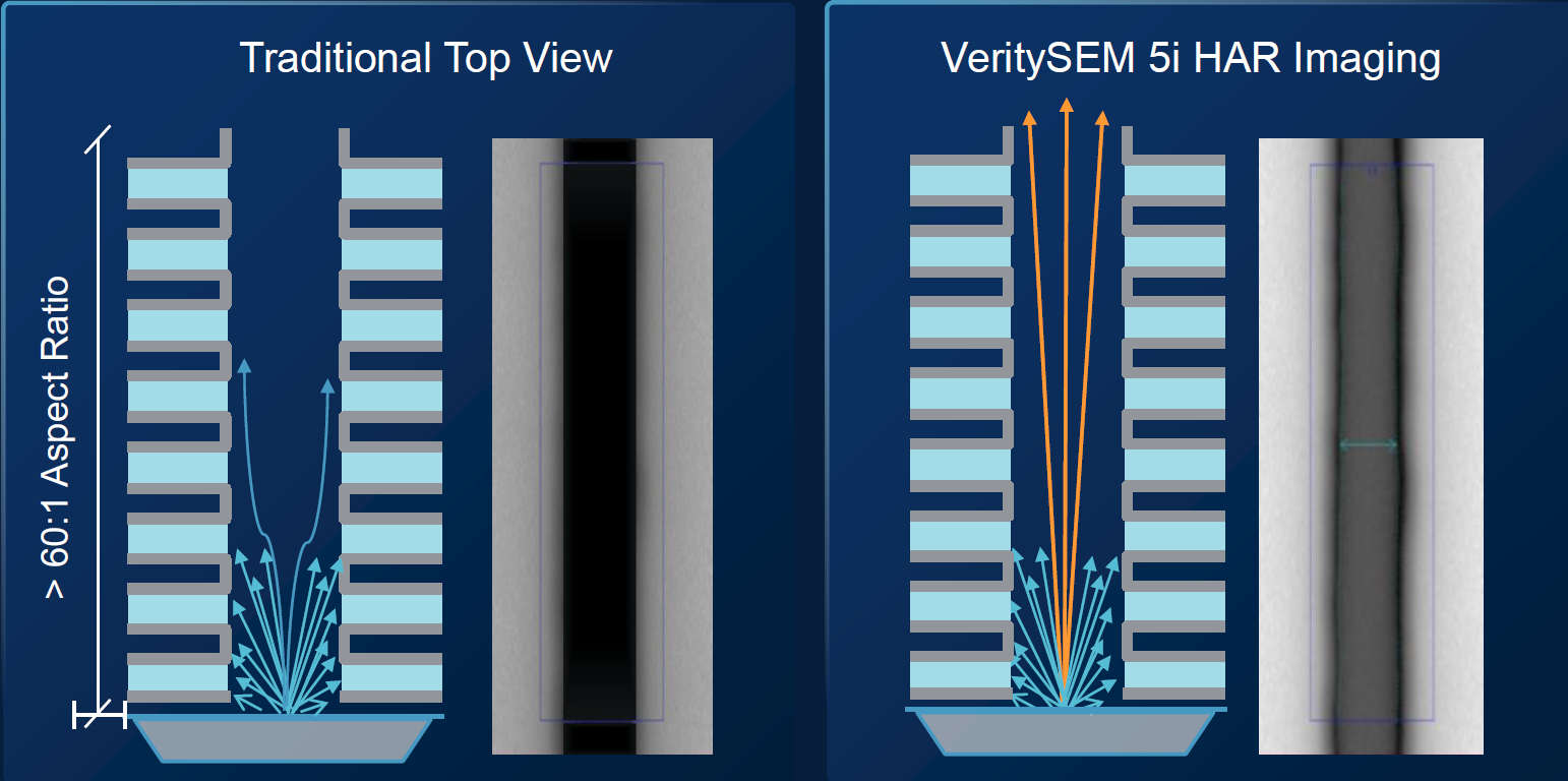
Meanwhile, a different approach was required for peering into deep holes. To understand their solution, we have to dig a bit into how SEMs work. At energies under 50 eV, a SEM measures so-called secondary electrons. These aren’t electrons from the source; they’re emitted by the surface atoms in response to interactions with the source electrons. While you can get back almost as many electrons as you shoot in with this approach, it doesn’t work well for these holes because the secondary electrons tend not to make it all the way out to be detected.
Instead, AMAT uses a “low-loss backscatter” (LLBS) approach, which provides returning electrons above 50 eV. This is literally about electrons on the rebound – when you detect these, they are electrons from the original source beam. Problem is, few electrons bounce in that manner, and fewer yet make it out of the deep hole – less than 0.1% – so it takes high sensitivity to detect them (as illustrated in the following figure).
(Image courtesy Applied Materials)
They refer to this as “high-aspect-ratio (HAR) imaging.” And the figure as shown omits one problem: the source is so bright that it blinds the detector to the dim stream of backscattered electrons. They end up having to do some fancy filtering to get the image they want.
They illustrate the results they see with in-trench vias below.
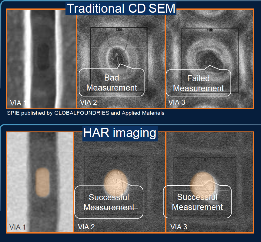
(Original images courtesy Applied Materials)
This is all part of their new VeritySEM 5i metrology system. They say that it’s the only high-resolution 3D-capable SEM system suitable for in-line use.
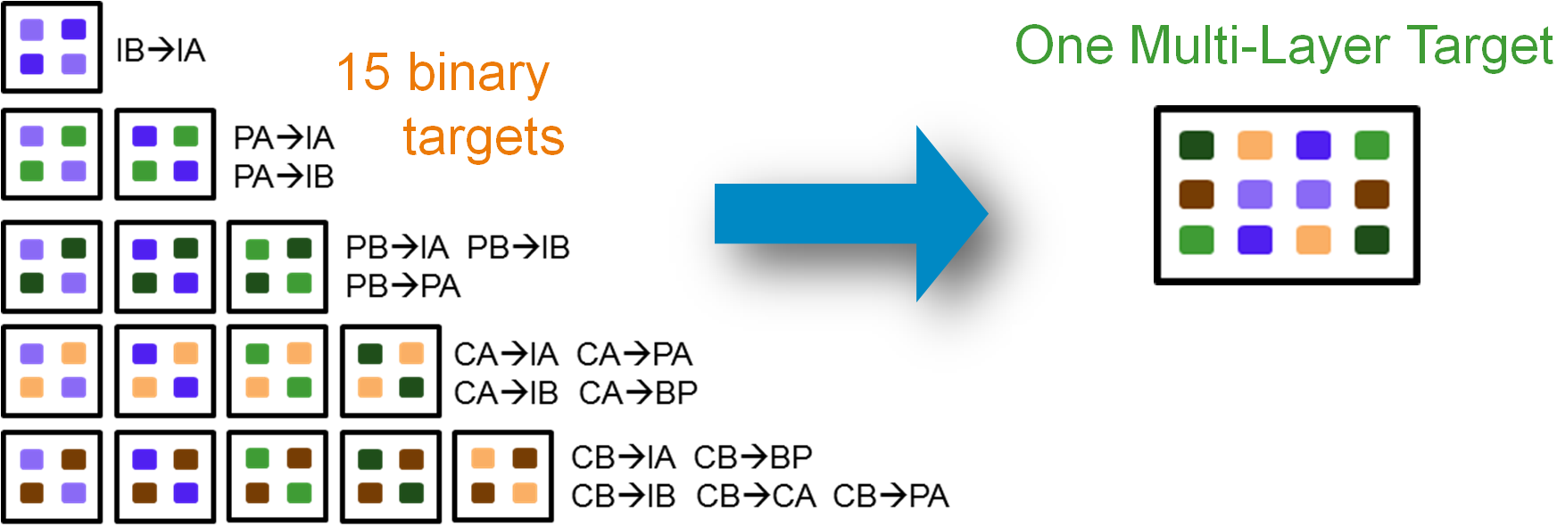
Meanwhile, KLA-Tencor is attacking a couple of different issues. One involves a redesign of overlay targets – two ways.
First, multi-patterning has created an overlay nightmare. Usually, one mask simply has to overlay properly on the prior one. But with multiple patterns, each of the partial-pattern masks has to overlay all of the other partial-pattern masks properly, and the combined sum of them all has to overlay the mask (or combination of masks) below them all. That makes for a lot of combinations and permutation in the overlay targets – which has made for many targets to get all of the combinations covered.
They’ve addressed this target proliferation with a single target that covers all the cases.
(Image courtesy KLA-Tencor)
The other redesign is more radical: it uses a completely new approach. They place gratings over gratings, with a slight built-in offset. The resulting diffraction patterns contain overlay information.
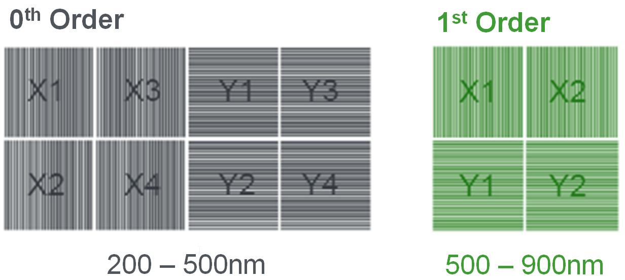
(Image courtesy KLA-Tencor)
One of the benefits of this system is the smaller target. Not only can it fit into a 40-µm scribe line, it can literally be put inside a die so that particularly sensitive areas can have overlay set and measured right nearby.
This is now handled by their Archer 500LCM system. Feeding results back to the scanner can help to bring overlay into better control as a part of their overall 5D integrated approach.
Finally, they’re upgrading their SpectraFilm LD10 system so that it can measure all films (thick and thin) in all configurations (single, few-, and many-layer). Thin layers tend to be used in stacks – most commonly NO, ONO, and SiGe. Thick layers might be used alone – oxide and photoresist are common examples – but they’re also being layered; anti-reflective coatings over oxide and ultra-low-? stacks are examples. And films are being stacked big-time in 3D NAND structures.
They want one metrology system that can be used for checking any of these configurations – and that means a wide range of spectra. They can go from deep UV, which they can use for ONO stacks in the range of 50-60 Å, to infrared, which they would use to penetrate a 3D NAND stack.
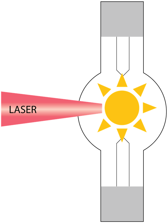
The element that gives them this capability is their new light source (briefly identified as being “brighter than the sun” in a prior piece). It’s now included in the SpectraFilm LD10. What’s different about this source is the way the Xenon plasma is maintained.
Ordinarily, you run a current to light up the bulb and then maintain the current to keep it lit. Problem is, this sputters the electrodes over time, which, in addition to eroding the electrodes, creates a metal haze that reduces illumination (and, presumably, the purity or integrity of the spectrum that makes it through). It also causes the plasma to move about in the tube as the sputtering evolves.
To solve this, they now use current to get the thing lit, just like before, but once it’s going, it takes less energy to maintain – and they use a laser for that, shutting down the original current. This means less current over time through the electrodes, saving on the sputtering.
(Image courtesy KLA-Tencor)
So we have a wide range of new solutions, all of them aimed at solving the problems inherent in trying to see vertically instead of just horizontally.
More info:
Applied Materials VeritySEM 5i


Will these advances for measuring 3D structures on wafers solve your aggressive-node metrology challenges?