

OK, so you’ve got this hole. A really deep hole. I mean, reaaaaally deep: some miles, perhaps. And you’d really like to know what’s down there, at least gas-wise.
Problem is, there could be lots of different things down there. You want to cover a wide range of substances – say, a hundred of them – with a single sensor to get some answers faster.
Oh, and there’s one more thing: as your sensor drops down into the hole, it’s going to pass through all kinds of materials and metals and whatnot. That’s going to play havoc with any electrical signals coming back up telling you the answers. Besides, it’s hot down there – most electronics won’t do well anyway. So… yeah, no electronics. How’s that going to work?
Contrived problem? Perhaps, but only because it abstracts a real problem that real companies have sensing the environment in areas hostile to electronics. This down-hole scenario could definitely apply to mining and oil-exploration applications with little added context.
The essence of the problem lies in detecting substances using an approach that allows, but doesn’t require, electricity. It’s one for which an Australian company, Panorama Synergy, says it has a solution, which they call LumiMEMS. Today we’re going to take a look at how they do this.
We’ll start with the basic tool that they employ: a MEMS structure – typically a cantilever or micro-bridge. Cantilevers have been preferred for this kind of application in the past because they move more than micro-bridges do, and so they’re easier to sense. But the technique we’re going to discuss is said to be sensitive enough to work with micro-bridges as well.
Is there a difference between the two, from a practical standpoint? We’re going to be bouncing light off of the bottom of the structure and capturing the reflection. The benefit of micro-bridges is that they remain flat, and they therefore reflect all light back at an angle consistent with its arrival angle. Cantilevers bend, changing the angle of reflection.
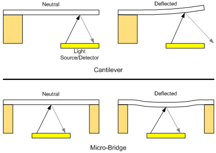
Figure 1. Both cantilevers and micro-bridges can be used as detectors, but micro-bridges return slightly more light.
But this is a detail that may or may not matter for a given application; either can be used. In fact, what we’re going to discuss can be implemented with any number of structures besides just cantilevers or micro-bridges, so we’ll focus on cantilevers simply because they’re easy to visualize (and draw).
Light is how the position of the cantilever can be detected. This is done by running a photonic waveguide underneath the cantilever, with a grating* that peels off some of the light to reflect off of the bottom of the cantilever; the reflection is then re-integrated into the waveguide. Critically, some of the light remains within the waveguide. (Refer to Figure 2 for an abstract view.)
This means that there are two light paths – the one that exits and returns and the one that doesn’t. The former is a longer path. So when it re-enters the waveguide, it will interfere with the light that stayed in the waveguide. That interference is determined by the gap distance between the waveguide and the bottom of the cantilever, and it can detect exquisite changes in that gap distance.
In order for this to work, the bottom of the cantilever must reflect the light well. So a highly reflective metal is used there. But, in order to get a controlled curvature, we need a “bimetal” strip – just like what used to (still does?) run the blinkers in your car. In that case, one layer expands more with temperature than the other, forcing a curve. In this case, it’s not two metals, but SiN over metal, and the internal stresses, which can be carefully tailored through the thicknesses, determine the curvature.
Those stresses can be impacted by materials that stick to the top of the cantilever. If there are particular materials that you’re trying to detect, you can “functionalize” the top of the cantilever with some material that has an affinity for what you’re trying to detect. If that material lands there and adsorbs, then it changes the stresses and the curvature.
There are actually two ways of detecting a substance. One is “statically,” using the approach we just discussed – measuring the gap distance. The other is dynamically, which focuses on the resonant frequency of the cantilever. The idea is that you pull the end of the cantilever down and then release it to let it vibrate down – like plucking the end of a mouth harp. You can pull it down – i.e., actuate it – by adding some electrodes below the cantilever in an area where there isn’t any grating.
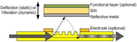
Figure 2. A side view of the waveguide running under the end of the cantilever, measuring the gap through interference of two light paths. The cantilever is a SiN/metal bilayer, with an optional functional layer on top for adsorbing some targeted substance. Electrodes for actuation are also an option.
“Aha!” you say. “But that takes electricity to activate the electrodes!” And you’re correct; this approach can’t be used exactly like this in a no-electronics setup. But they have a second trick up their sleeve: This technique is sensitive enough to detect random Brownian deflections (and remove them from the results). Because there will always be some amount of this random “twitching” of the end of the cantilever, it can be used to measure the frequency without explicit actuation. Yeah, it’s more delicate and slightly less deterministic, but it provides an actuation mechanism that requires no electronics.
Of course, the signal from dynamic mode will be more complex than that obtained from static mode because the gap is changing at a rate unrelated to the light frequency: it’s related to the resonant frequency of the cantilever. The resulting signal is a light beam that acts as a carrier modulated by the signal created by the vibrating cantilever.
The resonant frequency of a cantilever made out of a given material is determined by its geometry. Practically speaking, given cantilevers of the same construction (i.e., thickness) and width, the length becomes a “knob” by which the resonant frequency can be controlled (a point we’ll return to shortly).
Higher-order vibration modes can sometimes provide better sensitivity, but they have apparently been too tough to detect using past methods. According to the team, this new approach can be used to tease out those high-order modes.
There is one other catch: because of periodicity, there is a limit to how much gap can be unambiguously measured. As the gap opens, the interference pattern will go through a cycle of changes – and then restart that cycle. Beyond that point, the interference patterns from this wider gap look just like the ones from the narrower gaps of the previous cycle.
One way of addressing this, if it becomes a design issue, is to have multiple gratings under the cantilever, moving towards the anchor, so that you can measure the actual shape of the bend and disambiguate the measurement from the end.
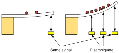
Figure 3. Extra gratings can help to disambiguate gap measurements if the range of possible gap distances is too wide.
So far, we’ve equipped a single cantilever with the capacity for sensing a substance either statically or dynamically. But what about a large number of substances? Well, you do that by creating an array of cantilevers, each of which has different functionalization. But… how do we tell one cantilever from another? Here’s where things get interesting. We’re going to do some serious frequency dividing here.
Let’s say we have 15 cantilevers arranged in 3 rows, 5 cantilevers per row. The first thing that happens is that the light is subdivided into three frequencies using wavelength-division multiplexing (WDM); this can be done optically and doesn’t require electronics.
So now we have three different optical carriers, one per row. Each of those carriers will be modulated by its cantilever signals. But there are five cantilevers on a row; how to distinguish them? Again, by assigning frequencies. Except that here we’re not going to divide the carrier; we’re going to assign frequencies to the different cantilevers – by adjusting their lengths, giving each cantilever a unique resonant frequency.
But it’s more complicated than simply looking for that frequency, since the resonant frequency will be changed by any adsorbed material. The higher the concentration of what you’re looking for, the more will adsorb onto the cantilever, lowering the resonant frequency (basically, it’s getting heavier).
That means isolating a band between the unloaded frequency and the “fully loaded” frequency for each cantilever. All of these signals modulate onto their carrier, and that carrier is then muxed back together with all the other carriers and is sent out as a single optical mish-mash of signals. In an all-optical setup, this would go out onto fiber to travel to some other location, like up at the surface above a deep hole, where electronics would be employed to tease apart the components of this signal.
With lots of cantilevers, this would sound like quite the challenge. But when dissecting the full optical mixture of signals, you still have both optical and electronic means to help out. So once the fully-mixed optical signal is retrieved, they first demux it into the different optical carrier wavelengths, each of which carries the signals from a single row. Each of those goes to a different photodiode, leaving each path with the simpler task of detecting only the bands for each cantilever within a row.
If you’re trying just to assay whether a material exists as a yes-or-no answer, then you can look around the unloaded and loaded frequencies to get a digital answer. But you can also approach it as an analog question, identifying the actual frequency and using that to report not only the presence, but also the concentration of the substance.
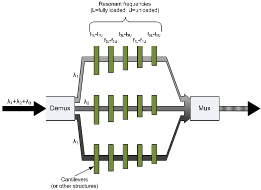
Figure 4. Three wavelengths of light are split into three different rows. Each row has five cantilevers, each with a different length and resonant frequency (loaded and unloaded). The results are mixed for analysis elsewhere. (Note: conceptual figure; nothing is to scale.)
The approach we’ve looked at so far operates in the frequency domain. If dynamic mode is being used with electronics, then, alternatively, you can use time-domain multiplexing (TDM) to assign each cantilever in a row a time slot for actuating and ring-down measurement.
While a chip like this can be made, for the most part, using standard IC and MEMS technologies, there’s one aspect of manufacturing that isn’t as obvious: functionalizing the cantilevers. That means putting a different material down on different cantilevers.
Strictly speaking, you may not be individualizing each cantilever. You might leave some unfunctionalized as references to correct against temperature or other drifts. You may also use multiple cantilevers for each material to be detected so that you can refine the result statistically. Nevertheless, conceptually, you could have dozens – eventually, hundreds – of different functionalizing materials that need to be applied.
Now, in the chip business, the standard way of doing this is to mask out unwanted areas to isolate those regions where the functionalization is to be applied. But there are a couple of problems with this:
- Adding dozens or hundreds of mask steps to fabrication isn’t going to make any bean counters happy. At all.
- It would have to be done before the MEMS release, and the release process doesn’t play well with many of the functionalization materials.
This means it has to be done some other way, post-release. Panorama Synergy has a number of different tools they can use to complete this final step, including inkjet printing (femtoliter droplets with micron accuracy) and the use of microfluidic channels on-chip for guiding a reagent to specific cantilevers.
They’re also looking at “dip-pen nanolithography” for possible future use. Think of this as “Honey, I Shrunk the Quill Pen.” An atomic-force microscope tip is dipped into the functionalizing material and then can be touched down on the cantilever with resolution under the 100-nanometer level. Sounds like you could even draw your signature on the cantilever with that level of accuracy.
I’ve been pretty generic in my descriptions, since my main intent has been to give a qualitative feel for how this works. For those of you curious about some of the details, the optics were built on SOI, with 2000-nm buried oxide (BOX) and 230-nm thick epi. The light they used in their early work had a 1550-nm wavelength, and the grating was 11.0 µm long in a 4-µm waveguide, with 610-nm pitch and 50-nm depth. The cantilever overlapped the grating by 1 µm on all three edges.
You can get yet more detail via two papers done through collaboration with the University of Western Australia. One deals with the details of a single cantilever; the other with an array of micro-bridges (both behind paywalls).
*We’re going to talk more about photonic components in an up-coming piece.
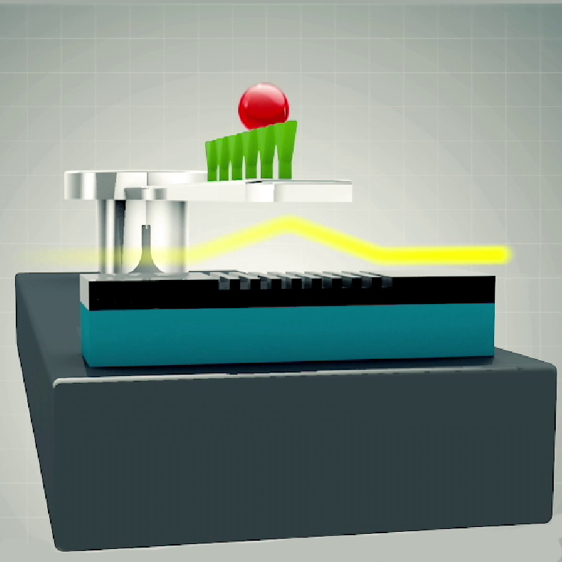
Cover image courtesy Panorama Synergy


What do you think about the possibilities for an array of substance detectors that doesn’t require electronics?
Finally, a condenser location that won’t saturate! Why, the sooner we can improve the VOC condition of the mineral environment by running an all-photonic control loop plant, the sooner we can mine and do pressure and height-mass based energy storage miles from the surface. J. Lightwave Technology (IEEE joint with OSA) and Photonics Technology Letters…