

It is a truth universally acknowledged, that an SoC in possession of well-verified IP, must be ready for tape-out. With due apologies to Jane Austen, this “truth” is more fantasy than fact. Of course, the IP components that make up a system-on-chip (SoC), whether from internal or external sources, must be thoroughly verified. However, this does not imply that simply plugging together well-verified IP will yield a functionally correct SoC. The “stitch and ship” approach introduces serious risks to an SoC project that can only be mitigated by a commitment to true system-level verification.
Too many SoC projects perform minimal verification on the complete chip. Verifying that each IP has been “stitched” in correctly is usually the first step. Formal analysis can be 100% effective at verifying IP and chip I/O connectivity. Unfortunately, most SoC teams do not go much further. Usually, they create a minimal testbench compliant with the Universal Verification Methodology (UVM) standard and run some basic tests –– confirming that a key IP block can read and write from memory or chip I/O pins, for example.
To invoke a cliché, this level of verification addresses only “the tip of the iceberg.” As a matter of fact, the iceberg turns out to be an apt metaphor for the challenge of SoC verification. As shown in Figure 1, there are many aspects of verifying an SoC thoroughly. The simplistic approach covers only those tasks above the water: formal verification of connectivity and simple testbench simulations to confirm that IP blocks are individually working. As with any iceberg, it’s the larger part below the water that presents the real danger.
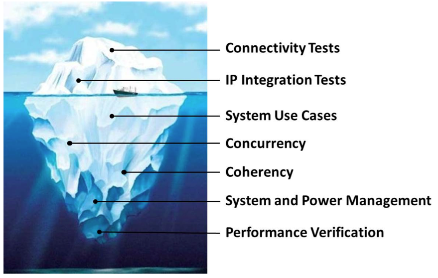
Figure #1 caption: The SoC verification iceberg includes formal verification of connectivity and simple testbench simulations to confirm that IP blocks are individually working, tasks that are above water. The more difficult tasks that reside below the water present the real danger.
Even if individual IP blocks are working correctly, they may not be interconnected properly to perform end-to-end applications representative of real-world use cases. In one notorious example, a bit-endian IP block and a little-endian IP block were connected together by a bus, resulting in the data being reversed. It is critical to test these use cases by stringing together multiple IP blocks into an application.
For example, for a digital camera SoC, it is not sufficient to verify that the imaging array can write an image to memory and the SD card controller can write an image to the card. The project team must verify that:
- A raw image can be captured and stored in memory
- The photo processor can read the raw image from memory, convert it to JPEG, and write the result back to memory
- The SD card controller can read the encoded image from memory and store it on the SD card
Similarly, as shown in Figure 2, the team also must verify that the stored JPEG-encoded image can be read off the SD card, converted back into a raw image, and displayed on the camera’s screen. Further, it may be possible for these two system-level applications to happen in parallel. The verification team must determine possible concurrency in the SoC and run tests that exercise parallel paths. These tests may introduce coherency cases in which caches or memories must be kept synchronized. It is critical that these cases be verified thoroughly as well.
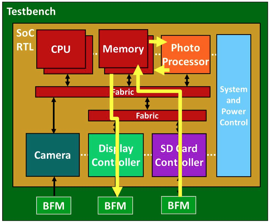
Figure #2 caption: A digital camera SoC supports data flows for multiple end-user applications, in this case, displaying a previously stored photograph.
Beyond regular modes of operation, SoCs have system-level functionality overlaying the applications. Most large chips have multiple power domains to conserve energy. It is essential to verify that powering regions of the chip on and off does not break the intended functionality. For example, turning off the camera while reviewing existing images from an SD card must work properly, but the camera must turn on again cleanly when new photos are to be taken. Some SoCs have security domains limiting which resources can access which other resources; these must be verified in a similar manner.
Finally, it is valuable to be able to assess an SoC’s performance characteristics in simulation in order to identify choke points in buses structures, memories, or I/O channels. This allows under-designed portions of the chip to be identified and rectified early in the project. A verification strategy that spans the iceberg by running multiple concurrent tests under system-level scenarios provides sufficient stress on the chip to measure real-world bandwidth and latency values for critical resources.
The question is how an SoC team can generate the tests necessary to cover all aspects of verification shown in Figure 1. This is impossible from a UVM testbench; manipulating the chip inputs alone does not provide the fine-grained control needed to set up complex applications and system scenarios. Since the power of an SoC lies in its embedded processors, it seems clear that these processors should be leveraged for verification. In fact, many SoC projects include a small team of programmers writing embedded tests to verify specific parts of the chip.
However, there is no way that even the smartest software team can hand-write the level of tests needed to avoid the iceberg. Hand-written tests might, at best, exercise a single IP block in a driver-level scenario. In the case of the digital camera SoC, one test might verify that the display controller can read an image from memory and write it to a testbench model of the display. Another test might verify that the SD card controller can read an image from memory and write it to a testbench model of the SD card.
The SoC cannot be thoroughly verified unless the complete end-to-end application scenario shown in Figure 2, and many others, are exercised. Very few SoC verification teams write application-level C tests. Those who do write single-threaded tests to run on a single embedded processor. Humans are not good at thinking in parallel, so writing code that runs in a coordinated fashion across multiple threads and multiple processors concurrently is impossible. Much as the UVM provides testbench automation for IP blocks, an SoC-level solution is needed to automate tests running on the embedded processors. Figure 3 shows how such a solution might work.
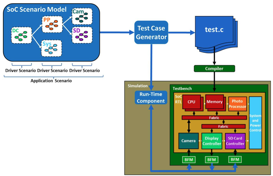
Figure #3 caption: Automatic generation of SoC test cases ensures
concurrent stress-testing of every aspect of the SoC.
The key to this approach is a sophisticated generator capable of producing multi-threaded, multi-processor, self-verifying tests that stress the SoC design. These test cases must run multiple application scenarios concurrently, exercising all the parallelism in the design. This level of verification finds deeply buried corner-case bugs and enables performance measurements of the system under stress. The test cases should be generated in C, since this is the most widely supported language across different embedded processors.
Processors may be homogeneous or heterogeneous; their architecture does not matter. Generated C test cases are compiled, loaded into SoC memory, and run on the embedded processors using the same flow as hand-written tests or production code. Thus, the verification team is operating within a familiar development environment. Test cases must run on “bare metal” without requiring an operating system to be installed. This implies that the test cases must handle directly such system-level functions as memory management and interrupt handing.
The two application scenarios discussed previously for the digital camera SoC both require data to be supplied to the chip and received from the chip. Many end-to-end scenarios have this same requirement, so it is not sufficient to generate test cases that stimulate activity only within the SoC. A run-time component is needed to coordinate the test cases running on the SoC with its inputs and outputs. In the scenario shown in Figure 2, the test case notifies the run-time component when a JPEG-ended image is to be supplied on the SD card inputs. It also notifies the run-time component when the raw image is to be read from the display outputs and compared to the expected result.
Finally, the run-time component should leverage existing verification IP (VIP) in the testbench to communicate with the SoC input and outputs. The VIP might range from a simple bus functional model (BFM) to a full-fledged verification component (VC) compliant with the UVM. This reuse leaves the details of the I/O protocols to the VIP that already handles it, enabling generation of higher-level and more efficient test cases.
Clearly, this approach puts a significant burden on the generator. It must “know” how to control individual IP blocks for driver-level functions and how to string the blocks together for application scenarios. Experience has shown that the best way to describe the SoC’s intended behavior to the generator is to use a graph-based scenario model. This model documents all the possible ways that data can flow through the chip to produce application scenarios. The generator can analyze the graph to determine these scenarios and which ones can be run in parallel in order to produce the multi-threaded, multi-processor test cases.
The scenario model can be produced by SoC system architects, designers, or verification engineers. It is hierarchical, so the SoC model can be composed from models for the individual IP blocks. Further, the graph-based approach means that the models look like the dataflow-oriented block diagrams already used to document designs. It is important that constructing the models not require the engineers to learn any new language.
Generation of SoC test cases from scenario models is not a theoretical method; an example of a commercial solution is available today. As shown in Figure 4, TrekSoC from Breker Verification Systems automatically generates multi-processor, multi-threaded, self-verifying C test cases that exercise realistic applications and system-level scenarios for the SoC. Its input is a hierarchical scenario model that is easy to create and maintain through the course of the project. Its output is C code that can be compiled for virtually any collection of processors.
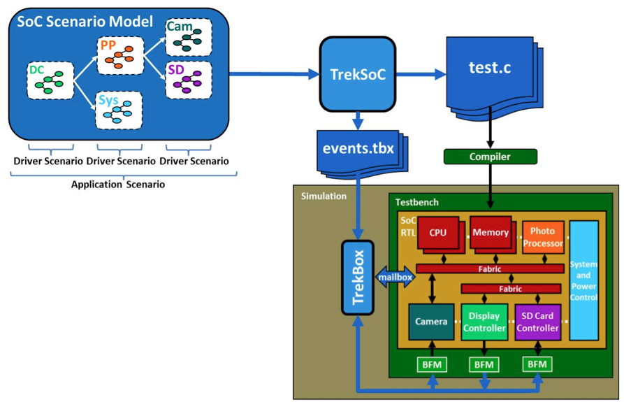
Figure #4 caption: TrekSoC fulfills the requirements for true system-level SoC verification.
The generator also produces an “events” file that lists the actions to be performed by the TrekBox run-time component. When a test case needs to supply data on chip inputs, read and check data on chip outputs, or print a message in simulation, it sends an event ID via a memory-mapped mailbox. TrekBox looks up the ID in the events file and takes the appropriate action, including leveraging existing UVM VCs in the testbench. This solution allows complete end-to-end applications, such as the earlier examples for the digital camera, to run concurrently and stress-test every aspect of the SoC.
Assembling a bunch of IP blocks, no matter how well verified, will not produce a working SoC without true system-level verification. The verification iceberg accurately describes the scope of tests that must be generated in order to thoroughly verify an SoC. Neither traditional testbenches nor hand-written tests for the embedded processors can come close to covering the iceberg. The only way to avoid its risks is to automatically generate test cases from scenario models. This approach has been in use for several years at industry-leading SoC companies, proven in tape-outs for dozens of chips that went to production on first silicon.
About Thomas L. Anderson
Thomas L. Anderson is vice president of Marketing for Breker Verification Systems in San Jose, Calif. His previous positions include Product Management group director of Advanced Verification Systems at Cadence, director of Technical Marketing in the Verification Group at Synopsys, vice president of Applications Engineering at 0-In Design Automation, and vice president of Engineering at Virtual Chips. Anderson has presented more than 100 conference talks and published more than 200 papers and technical articles on such topics as advanced verification, formal analysis, SystemVerilog, and design reuse. He holds a Master of Science degree in Electrical Engineering and Computer Science from MIT and a Bachelor of Science degree in Computer Systems Engineering from the University of Massachusetts at Amherst.


Breker’s Tom Anderson has looked at the challenges of verifying SoCs. What do you think?