

There’s an interesting twist on nano-scale electronics that’s being worked on at the University of Pennsylvania, and it has an optical element. Skimming over some of the coverage, you might think of optical circuits as something akin to photonics, where light is being shuttled around and manipulated. That is, in fact, not the case. To find out what this new field, with the proposed name of “metatronics,” is about, we need to go back to some basics. These aren’t all things we might be recalling from long-forgotten classes: some of these “basics” were discovered long after some of us left school.
First let’s touch on what is referred to as “plasmonics.” This has to do with the interaction of light and metals. Metals cannot support a sustained electric field because the electrons can move about like an electronic baitball; they swim wherever they need to in order to cancel out the applied electric field, like so many sardines avoiding sharks.
Of course, if you start varying the electric field, then this baitball moves back and forth in response. But electrons are physical entities, and they take time to move, and they don’t stop moving instantaneously. So if you start oscillating the field fast enough, they can no longer keep up. If a steady field were to be instantaneously removed, the electrons, freed from the field, would return to the ions from which they were stripped, but they wouldn’t just go there and stop: they’d overshoot and then get pulled back and overshoot again, although a little less, and so on, oscillating until damped out.
The natural frequency at which this oscillation happens is called the “plasma” frequency, and it tends to be in the ranges that we associate with light. Below this frequency, metals can’t transmit the electric field carried by photons because the electrons are able to respond quickly enough to cancel out the field, and so these metals reject and reflect all photons that impinge on the surface, making them highly reflective. This is why most metals, which have a plasma frequency in the UV range, reflect all visible light.
Above this frequency, the electrons are frantically trying to keep up (in vain). There are a few metals – gold, silver and copper in particular (so-called “noble” metals) – that have plasma frequencies within the visible range – some frequencies are transmitted instead of being reflected, giving the metals their characteristic colors. Such metals are referred to as “plasmonic”; others are “non-plasmonic.” (Such a description applies, however, only with respect to a given frequency.)
This interaction between photons and metals is the basis for the “optical” nature of our topic. It’s not that we’re going to be manipulating light: we’ll be manipulating electrons, but in new ways, and, rather than the source of electrons being a battery, it will be light that provides current – by jostling the existing electrons around at optical frequencies.
Things start to get interesting from here. But it’s bad news for those of us that ran screaming from all things Maxwell’s. There are two current components in Maxwell’s equations: one is the standard current that we work with at low frequencies; the other is the so-called “displacement” current. Ordinarily, we consider the displacement current only when dealing with capacitors: it’s what lets us envision a current going through a capacitor even though there are no electrons actually moving through the dielectric that separates the capacitor plates.
But, above the terahertz range, where electrons start to have a hard time keeping up with oscillations – and therefore can’t really move through a wire (because, just when they get started, they get yanked back), the displacement current dominates. Displacement current also flows in dielectrics; it’s just that the electrons can never leave their atoms; they simply vibrate about, moving ever so slightly off center.
Professor Nader Engheta at the University of Pennsylvania and his team of students have been envisioning small metallic nano-spheres at visible wavelengths. Using plasmonic materials like gold, you should be able to establish resonance – much like an LC tank – by shining visible light (above the plasma frequency) onto them. And so these little particles can act like nano-inductors (with an associated “fringe” capacitance that I’ll call “parasitic” so that I can conveniently ignore it). Non-plasmonic metals don’t resonate at that frequency; they look more like a C-C tank and therefore can act as nano-capacitors.
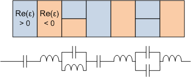
The key material property that ties into this all is the permittivity – or the ability of a material to “permit” an electric field, represented by epsilon (ε). The permittivity varies by frequency and is a complex quantity. If the real portion of the permittivity is positive, then the material acts like a nano-capacitor; if negative, it acts like a nano-inductor. The imaginary portion of the permittivity represents loss and provides nano-resistance.
The idea is that such particles can, conceptually, be combined to create nano-circuits. Rather than using spheres, you could build structures where the different materials abut each other in specifically-designed ways to effect actual circuits.
But there’s another catch when trying to build circuits like this. We can direct standard current in wires, routing it around bends and in any direction we want, because the wires are surrounded by non-conducting materials, confining the electrons. Displacement current, however, is not so well-behaved: it isn’t confined by the metal boundaries (as capacitors prove). So, when trying to build a circuit, much of the field (or, more importantly, the resulting displacement current) can “leak” uncontrollably into the surrounding materials. The current must be confined in order for us to direct its path.
The approach here is to use two different classes of material that are, again, related by permittivity. The permittivity determines how much displacement current a given field will cause. So if the real part of the permittivity is extremely small – near zero, yielding the name “epsilon near zero,” or ENZ – then the material won’t “permit” the field and will yield a very small displacement current – thereby acting like an insulator.
For the conductor, you can use a material where the real part of the permittivity is large – an epsilon-very-large, or EVL, material. A nano-cylinder of EVL material sheathed by a layer of ENZ material will look like the nano-equivalent of an insulated wire.
So… backing out a bit from this nano-morass, let’s look at a couple of higher-level concepts. First, let’s consider what we’re getting by doing this. Those of us that work well below the RF range get the convenience of treating electrical components as lumped elements. We put a resistor down on a board or a chip and we say that the resistor is confined to that specific location. This works because the wavelength of the electric signal is much longer than the physical dimensions of our components.
If we turn up the frequency, the wavelength comes down, and we can no longer lump our components: resistance and capacitance and inductance are everywhere. Tell that to a digitally-oriented guy like me, and, well, it just puts a shiver down your spine.
But these nano-structures are so tiny that, even at optical frequencies, they can be treated as lumped components, and you leave RF techniques behind, coming back to more accessible circuit design.
As to the name “metatronics,” this is something that Prof. Engheta came up with to reflect the fact that nature doesn’t give us everything we need to make this happen: we need “meta-materials.” These are materials that are specifically engineered to have properties that don’t exist in nature, like a negative index of refraction. We need to engineer the ENZ and EVL materials, for example, in order for this all to work.
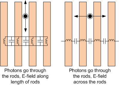
The team has demonstrated some of the concepts that this theory proposes. They created low-stress silicon nitride (LS Si3N4) “nano-rods” suspended in air, where the real part of the nano-rod permittivity is negative (at the frequencies they use), making them act as inductors, and the air gaps, having a positive real permittivity component, act like capacitors. The gap width and rod width are in the subwavelength range.
They were able to use this structure to evaluate two different kinds of circuit by polarizing the light differently. If the E-field was aligned with the rods, then the gaps and rods appeared to be in parallel; if polarized across the rods, then the components appeared in series. To make a long story much shorter, the results of their tests were consistent with this lumped view of the equivalent circuit.
So at this point, we have a concept and some initial studies lending some credence to the concept. The details of it all are much more involved than what I’ve gone into here, of course; I much prefer motivating through visual analogs (like the image of an oscillating electron) instead of by the tyrannical dictates of equations*. (“Why does it work? Because the equation says it does!”) But, of course, the actual work of wrestling all the equations and details to the ground, bringing the industry on board, and starting to build real circuits in a serious way remains to be done before this comes to a fab near you.
More info:
News release on first metatronic circuit
*OK, you got me… the truth is that the details hurt my head…


Are you itching for a metatronic circuit? What do you think about the concepts?