

It doesn’t usually happen this fast… or this slowly.
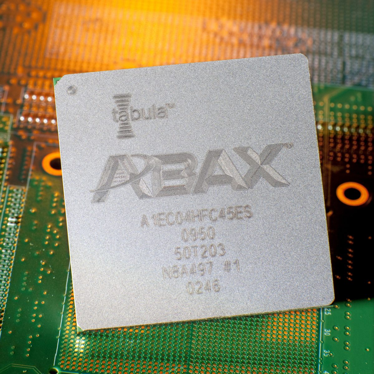
Tabula, who just a couple weeks ago announced their Spacetime 3D FPGA architecture (see our article here) has now followed up with product announcements for their new ABAX family of FPGAs. As predicted, ABAX comes in sizes (or size-equivalents) that are favorably competitive with current 40nm high-end FPGAs, and at very low prices. The A1EC04 devices (rated at .39 “MegaLUTs”) are expected to be sampling in Q3 and shipping in volume in Q4 of this year, at a price of $150 in orders of 2,000 units.
Yeah, that’s a lot of equivalent LUTs for not much money.
Let’s peek once again under the virtual hood of this Spacetime stuff and see what’s going on here. First, let’s notice that the entire family has identical I/O and packaging – 920 user parallel I/O with 48 6.5 Gbps Serdes in a 1936 BGA flip-chip package. Ditto the built-in RAM – 5.5 MBytes on all devices, regardless of size. In fact, almost all of the specs, apart from LUT count, are the same across all the devices in the newly announced family.
As you notice, the only thing that changes from device to device is the “MegaLUT” count – except that the biggest device – A1ED06 also comes with 1280 very fast (1.6GHz) Multiplier/accumulators. What’s going on with the LUT count? A lot, as it turns out. As we discussed before, there aren’t that many LUTs actually on the chip. If you looked under a microscope, you’d see only 1/8 that number of LUT-like objects. Tabula runs a very fast (1.6GHz) clock that rotates each LUT through a series of 8 different configurations, making the effective number of LUTs 8 times the number of physical structures.
While this may sound like cheating, Tabula certainly didn’t start the “effective LUT” scam in the industry. Xilinx and Altera have been running that one for years. First, each company claimed they had more efficient logic structures than the other, and began quoting their density scaled-up by some seemingly arbitrary factor to make up for the apparently-egregious architectural deficiencies of their competitors. More recently, they began quoting their densities in LUT4 “equivalents,” even though their devices no longer use 4-input LUTs. Tabula, with their 8X factor, however, has taken this abstraction to a whole new level.
Just about the only thing on the chip that isn’t “folded” with this 8x factor is, of course, the IO. Folding the memories and LUT structures has some interesting side benefits in addition to the higher effective density of the chip. These advantages fall out of the architecture and clearly create some trade-offs that will be important to understand using this technology.
First and most obvious is shorter interconnect. Since the chip is significantly smaller than a conventional FPGA with the same density, the interconnect is shorter – requiring less routing resources and giving a shorter average connection length. Instead of interconnect capacitance, most of the delay is around waiting for the folds to cycle – swapping a notoriously unpredictable delay for a perfectly predictable one.
These shorter routes also help with connecting to IO – particularly to high-speed serial transceivers. Instead of breaking out physical routes 1 bit at a time, you can have them routed in 8-bit bundles, making more efficient use of your physical routing resources. This also gives more predictable timing between IO and core, and in general will move wide datapaths around the chip in a more orderly fashion.
Memories also get a nice gift from folding. Since each physical memory block is time-multiplexed, we get the equivalent of 8-port memory for kinda-sorta the price of one. Memory configurations can be changed in real time (on a sub-cycle by sub-cycle basis), so those physical memories can be configured as wider and flatter (more bits with fewer ports) or taller and skinnier. Connecting them to neighboring logic is also easy since each bit can be aligned with the port of the memory that drives it.
All of these advantages are theoretical, of course, and rely on the compilers (synthesis and place-and-route) to actually take advantage of them. What we want is to design our FPGA the usual way, and have the magic of 8-way folding handled seamlessly behind the scenes for us. Tabula claims that their tools can do just that.
So – what are we giving up for all this? Well, first, it’s important to realize that the effective densities are reliant on 8 levels of folding. With the Spacetime clock running at 1.6 GHz, that means your user Fmax will have to be at 200MHz to get the most of the density. If you crank up the user clock, the folds melt away – you give up half of your density at 400MHz and 3/4 of it at 800MHz. Luckily, there is a high-degree of granularity so you can trade off folds for frequency pretty precisely, and different sections of a tile can run at different frequencies. The compiler supposedly handles this automatically, shielding us from the complexity of multiple folds in different areas, but don’t be completely taken aback if your density isn’t what you expect if you’re pushing the speed of your design.
Using this folding technique, Tabula claims overall advantages of 2.5X on logic density, 2.0x on memory density, 2.9x on memory ports, and 3.7x on DSP performance against conventional FPGA architectures on the same (40nm) process node. We expect that will come with some penalty on power consumption, although for the target audience of communications infrastructure designs, the increased density and lower cost may be more important than the absolute lowest power. To be fair, we’ll know more about the power when we see how ABAX performs in real-world designs.
If all those ratios are true, Tabula’s architecture gives something like a 2-process-node advantage over normal FPGAs. That will be important soon, as Xilinx and Altera have already both announced 28nm plans. Given Tabula’s apparent funding and determination levels, as long as they can stay within one process jump of their bigger competitors, they have a fighting chance – on technology at least. It’ll be exciting to watch!


