

Passing beyond a looking glass has been a useful metaphor for any topsy-turvy, head-spinning, when-will-this-trip-be-over, bizarro-world experience ever since Lewis Carroll bestowed it upon us. It’s that feeling that you’re stuck in a strange dream somewhere, where croquet balls unroll and run away, queens chop heads off willy-nilly (OK, to be fair, she didn’t chop them off… she had people that were supposed to do that), where what should make sense doesn’t and what shouldn’t does.
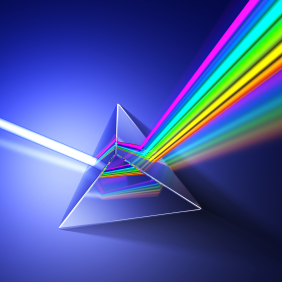
The looking-glass concept can be applied on three levels within the increasingly finely-dimensioned world of semiconductor design and fabrication. The first is the simple fact that quantum effects become important in this realm, and we all know that no world is more bizarro than quantum. The second is the fact that optics and the flow of light are key to the effective creation of ICs. While a looking glass implies reflection rather than transmission of light, the passage of light through glass becomes less and less trivial the further we encroach upon physical dimensions smaller than the wavelength of the light used to image patterns on silicon.
The third other-worldly relevance will resonate with those of us firmly planted in the everyday world of the time domain. Here we are dominated by cause and effect, sequentiality of events, and, in the context of light, wavefronts and interference and refraction in simple terms that can be conceived of in as banal an analog as the flow of ripples in a pond. Pass through the looking glass and you enter the world of the frequency domain, where events are merely implied and where we are surrounded by vibrations that obey no temporal strictures. Presumably, by making this shift, what seems convoluted in the time domain can be transformed into mathematics as simple as multiplication. But that’s the problem: it’s a trick of mathematics. It works because there are demonstrable results all around us. But “intuition” about the frequency domain is a decidedly learned characteristic, which means that, by definition, it is not at all intuitive.
We bring together the latter two elements of through-the-looking-glassness (with the former being imbued throughout this particular landscape) in a discussion of an announcement recently made by Cadence. It takes place in a realm usually hidden from the average IC designer, and yet one whose visibility is becoming more useful as the limits of lithography are challenged. It’s the world that dictates how the light from a source journeys to and through the familiar masks that selectively block light and create patterns on silicon.
Let’s start with the fact that we’re stuck illuminating masks with wavelengths of light that are longer than we want (at least until “EUV” arrives). One trick that can be used to “shorten” the wavelength is to exploit the fact that light contains “orders,” analogous to “harmonics” in the more tangible world. A brass player uses such harmonics as the basis for achieving a broad range of notes. The (false) fundamental, referred to as a pedal tone (which, if poorly executed, has the flatulent finesse of loose lips flapping in a hurricane) is rarely used, deferring instead to the higher harmonics, each of which, having a higher frequency, has a shorter wavelength.
By analogy, the first- (or higher-) order component of the illumination light will have a shorter wavelength – if this component can be emphasized, we can improve the printing quality of small, closely-spaced features. This is done by “off-axis” illumination: bringing the light in at an angle. The trick is, which angle? And for what part of the circuit? Lines going horizontally will benefit from light angled from top or bottom; lines going vertically will benefit from light angled from the sides. Of course, real circuits are a combination of all of these, and spacing and density also matter, so the best angle will be different all around the circuit. And yet, for focus purposes, the illumination pattern is generally best if symmetric.
This aspect of optical proximity correction (OPC) has traditionally (if anything about this fast-moving industry can remotely be considered “traditional”) been handled on an empirical basis by making available a series of standard “masks” for the source light. These aren’t masks in the traditional sense of selective blocking of light, but rather operate in the <cue eerie music> realm of frequency domain, diffracting light to improve the effectiveness of its delivery. The best pattern to use will depend on the circuit and has traditionally been chosen empirically from a set of pre-defined options. The options consist of such patterns as annular, bulls-eye, a broken-annular-looking pattern called C-quad, and others.
The goal of OPC is to make production as robust as possible in the presence of process variations, and the process window is typically “discovered” by experimentation and modeling. At the 22-nm node, Cadence – in a technology collaboration with Tessera – proposes to “construct” the window computationally as an element in an updated incarnation of OPC: “PPC”, Process and Proximity Correction. And a key to this is not to pick the best of a few pre-selected source mask options, none of which may be particularly good, but rather to design a custom source mask that will provide illumination yielding the best feature resolution over the widest process window for the given circuit.
The specifics of how this works – or indeed, why it works – is certainly vested with the power to make my head spin, as it immediately launches me into the frequency realm, accompanied by subtle hints of vertigo and nausea and a long lingering disoriented finish. Even if you’re comfortable with s-plane manipulations in the electronic context, the optical equivalents may still feel foreign since they’ve evolved out of a discipline distinct from electronics that has a provenance and a language all its own.
Basically, a customized source mask creates a specific holographic image that optimizes the placement of light on the die, kinda like placing more light where more is needed. But not exactly “where” from a conventional “where” standpoint… the concept of “where” is far too mundane for the frequency domain; think of whatever the Fourier transform of “where” is and you’ve got it. It’s a far more vexing mental circumambulation than parsing what the meaning of “is” is. Suffice it to say that the source mask reflects (in the virtual, not literal, sense) the Fourier transform of the layout. Nuff said.
The practical nature of what happens involves iteration by software that converges on a solution that will be used for a specific circuit. The optimizer does this using clips from the layout, an initial model, and information on the illumination depth of field, dose variations, and allowable edge tolerances; it generates an optimized illumination profile, optimized patterning masks, and resist thresholds. Edge placement isn’t calculated on an edge-by-edge basis, but rather on an entire area at once, further speeding the solution. The goal is to reduce the time required to achieve a wide robust process window – they’re touting first tapeouts a week or less from model availability, as opposed to 1.5 – 3 months. So far, convergence is quick, requiring only about four iterations. A comparison with non-customized illumination indicates wide process tolerance with improved focus.
Of course, at the 22-nm node, it will be some time before your average designer needs to think along these lines. This is a couple generations down the line from where aggressive production designs are being done right now. But it provides some visibility into the kinds of issues that are being resolved in a world where dimensions are shrinking but exposure wavelengths aren’t. It gives you some time to prepare, to gird up, to have that virtual – or literal – drink in preparation for a wild ride.
As for me, I’m going to back away from the looking glass and reintegrate with the everyday world, where events occur with beginnings and endings, and where I can be measured more by the content of my character than the content of my frequencies.
Link: Cadence announcement


