


The mood was dramatically different from prior years. Hope was in the air, and there was a distinct sense that the long sought-after achievement might actually be within reach.
If I tell you that the venue for this altered state was the SPIE Advanced Litho conference, then you can probably guess what I’m talking about: EUV. (OK, that and the spoiler title…) The tenor of the presentations, and even comments from the audience, were completely different from last year and prior years.
EUV has been discussed as the next big lithography step since I started my engineering career. With it having started that long ago, you would think that it was far enough in advance to put it in place in time for when it was needed. But it turned out harder than anyone thought, and, instead of EUV, we had things like immersion (for a better effective numerical aperture, or NA) and all the optical correction tricks played so that we can print far smaller features than we really should be able to. Necessity’s maternal nature, and all that.
The last few years have literally held a barely stated question: will EUV even be ready before it’s obsolete? The big focus was on source power, which had been inching up too slowly (with one year reporting something around 50 W and the next year reporting more or less the same number, “only this time we mean it”). But there have been numerous other issues in the way: resists with good exposure and line-edge roughness characteristics; inspection technology; masks and pellicles; the entire ecosystem, really.
This year might be characterized, by contrast, as being a huge sigh of relief. We’re not there yet, but, for the first time, the crowd seemed to have a distinct sense of, “This is going to happen.” That’s a big change. I checked my impression with a few other people, and it wasn’t just my imagination; they agreed.
Past conferences tended to report a few modest bits of progress and then a laundry list of things that still needed working. This year, it was a laundry list of things that work and a dramatically smaller punch list of things to fix. Success isn’t right around the corner, but it finally feels like convergence.
A Shorter To-Do List
So let’s talk about the issues that remain, since that’s now the shorter list. To be clear, there are three different ASML models out there. The first one to ship (selectively) to customers was the NXE 3300; then work was shifted to the NXE 3350, and the NXE 3400 is due for delivery by the end of the year. Reporting various performance numbers gets a bit confusing, since the different numbers may come from different machines.
My approach here is not so much to draw clear distinctions between the machines, but rather to report on what appears to be possible with whichever machine. Ultimately this all comes together when EUV is inserted into mainstream commercial flows – which is a couple of years out — in 2018.
The first topic is, of course, as always, source power. There have been dramatic improvements in power, although the required value seems to have crept up again to 250 W. ASML says that they’ve demonstrated 200 W with good dose control, so it’s close. Critically, there appeared to be confidence that this can be done – in contrast to prior years.
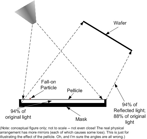
A caveat to this came up in a subsequent discussion I had with Mentor Graphics. Andres Torres noted that, with the advent of pellicles, more energy is lost due to the pellicle, possibly necessitating an even higher power level to compensate.
These pellicles are effectively sneeze-guards put on the masks to block so-called fall-on particles – that is, defects that aren’t an intrinsic problem with the mask, but rather are dust or something else in the environment that falls onto the mask. The idea is that a pellicle, rather than the mask, catches the particle, and the pellicle is far enough from the mask to keep the particle out of focus so that it doesn’t print.
Pellicles are a regular part of standard lithography and have been for years. But EUV poses new challenges – the primary one being that the optics are all reflective, not transmissive. So wafers aren’t patterned by light shining through a mask; they’re patterned by light bouncing off the mask. So… if you put a pellicle of the wrong material in the way, you risk all the light bouncing off that instead.
They have managed to come up with pellicles, however, made out of polysilicon or other materials that are as transparent as possible to EUV light. Even so, you lose 6% in both directions – meaning that when the light travels to the mask through the pellicle, 94% of the light gets to the mask. It then bounces off and goes back through the pellicle – or at least 94% of the remaining light does, anyway, and arrives at the wafer. That cuts the original light intensity to 88% of what hits the pellicle on the first pass, which is why more power might be needed.
Machine availability or uptime is still not as high as needed. It’s one thing to prove that the machine can achieve a certain power level; it’s another to do that day in and day out, with minimal downtime. The older ASML NXE 3300 unit, in place at a number of customer sites, has been running around 800 wafers per day, with more than 300,000 wafers exposed so far. Uptime is in the 75% range, with 10-15% of the downtime being unscheduled. That’s an area of focus.
Part of this downtime comes from the droplet generator used to drip molten tin into the reaction chamber (wherein those droplets are blasted with the awesome laser cannon). Tin is apparently a fussy metal to work with, but they’ve managed to double the tin supply “lifetime” to a month while also shortening the downtime required to swap out the unit.
Meanwhile, they’ve done better protecting the collector against haze and debris. They’ve gone from a hazing level of 0.7 %/gigapulse back when the power was at 40 W to 0.4 %/Gpulse at 125 W. Hydrogen helps with this process, something we discussed last year.
Resist is still another matter being resolved. You might remember that last year we looked at Inpria’s new metal-oxide resists. Talking to others at the time, I got the distinct impression that Inpria had a lot of credibility-building to do. Well, this year, everyone was talking (favorably) about their results using the Inpria resists in place of standard “chemically amplified resists,” or CARs. They were everywhere. There’s still work to be done, in particular to raise the sensitivity.
And there’s another type of resist being considered: one that has nanoparticles in it. Again, the idea is to find materials with low granularity (for smoother lines) and high sensitivity so that they can boost throughput (and take pressure off of source power) by getting away with shorter exposures. I may spend some time covering this in more detail in the future.
Another development is the announcement of a new high-NA process. By changing the magnification and the aperture, it looks like they can go from a 0.33 NA to 0.55. But it requires a so-called anamorphic lens – magnifying by 8x in the horizontal direction but 4x in the vertical direction. This topic may also be good fodder for a future deeper dive.
The final big thing I’ll mention is actinic inspection of patterned masks, something that exists for standard processing, but not for EUV steps. “Actinic” means that it’s inspected using the same light wavelength as is used for exposure. The idea is that some defects are visible at different wavelengths, and the only thing you really want to focus on (sorry) are those defects that will matter during exposure. In other words, those that are printable at the EUV wavelength.
Last year we looked at an EUV source for actinic inspection, but you need more than a source; you need a full platform. ASML mentioned that, to date, KLA-Tencor had “shown no interest” in building such a system. Since they have a dominant position in the inspection business (we’ve looked at new releases over the last couple of years), it’s natural that folks are going to look to them for help.
I checked in with them, and Sr. VP David Fisher said that, “Due to the small size of the mask market and the large investment to bring the product to market, KLA-Tencor proposed a shared funding model with key customers, however there was not enough interest at that time to develop the product.” In a keynote, Intel noted that, “The current lack of commercial Actinic Patterned Mask Inspection (APMI) is not a show-stopper, but without it, yield and cost may be an issue.”
So that’s a 40,000-ft rundown of progress. The highest-level summary is that EUV now appears to be more of a statement than a question. Critical dimension uniformity and overlay performance are said to meet the needs of the 7-nm node, although full production looks to be more like the 5-nm node.


Are you satisfied that EUV will happen in time to be useful?
It is a very nice summary, thanks. I would say the attitude is positive rather than the outlook or mood or tone. Objectively, from the reports by customers, there are still many serious problems with EUV so that it’s behind even for 10nm. Although the most natural timing now is 5nm, the gap is still very wide.
Agreed; a matter of semantics, I think. The big change isn’t that everything is fixed, but that, for the most part, it feels like it’s going to happen.
Reading the papers after the conference, I get the feeling it’s not going to happen.