

Wow, here it is March, and there’s still more to talk about from IEDM. That said, this will wrap it up – just in time to enter the new conference season.* We round up our coverage by surveying some of the MEMS and NEMS ideas presented.
MEMS was the darling topic a couple of years ago, when every few weeks heralded some radically new MEMS structure or approach. That pace seems to have slowed as winners and losers have shaken out (or are still battling), and the spotlight has moved as we’ve become accustomed to the idea that we can build ridiculously tiny mechanical instruments as if by magic. So newer papers tend to reflect optimizations – mostly.
NEMS, on the other hand, is still waiting in the wings – its time hasn’t really come yet, it would seem. MEMS has lots of life left before it yields to its thousand-fold shrink. And yes, there are qualitative differences in the NEMS world – it’s not “just the same old thing, only smaller,” as we’ll discuss.
I’m mostly going to hit highlights and dwell on main points rather than digging deep. You can find the nitty-gritty in the IEDM proceedings – mostly within session 22 (plus paper 8.1).
Thermal resonance (22.2)
We’ll start with a sensor that does take something of a different physical approach. It turns out that the thermal, mechanical, and electrical properties of some piezoelectric materials can create sustained internal oscillation. You run a DC current, which heats (and distorts) the material, which raises the resistance, which reduces the current,… which reduces the effects until you come back to the starting point. That’s my ultra-high-level take on it, anyway.
The problem here is the obvious one: power, as expended in that pesky DC current. Additional work had been done to show that you could reduce current by shrinking the element to one (or more) small beams, but that also raised the resonant frequency. What was done in this paper was to craft a resonator shape that decoupled the beam size (and hence the current) from the resonant frequency.
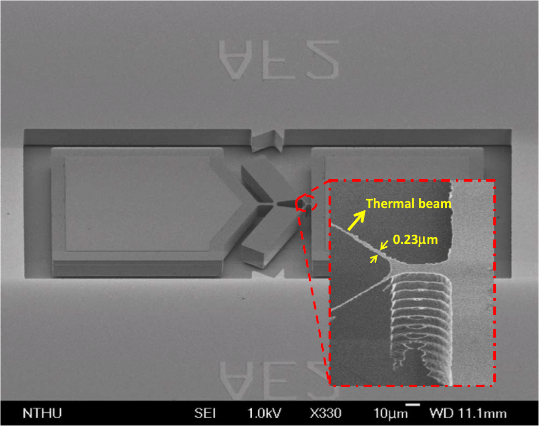
The result was a 70-µW resonator, with a Q over 6000. They noted that this isn’t the highest-Q resonator out there – you can find ones with Q in the 50,000 range, but it takes 4.5 mA of current to get there.
The paper is, “A Self-sustained Nanomechanical Thermal-piezoresistive Oscillator with Ultra-Low Power Consumption,” Kuan-Hsien Li et al, Institute of NanoEngineering and MicroSystems, National Tsing Hua University, Hsinchu, Taiwan
Monolithic 9-Axis (22.6)
The next topic was claimed to be a first. Yes, you may object that we’ve had 9-axis sensors for years now, which we have. But the difference here is “monolithic”: all nine sensors, including the magnetometers, are built on the same silicon-on-insulator (SoI) wafer using no magnetic materials.
They did this by using Lorentz-force magnetometers. These exploit the fact that a coil running a current will bend slightly in the presence of a magnetic field (even a weak one like that of the earth).
Having all of the sensors on a single substrate with no exotic materials reduces costs and, critically, means that all of the 9 sensors will be mutually aligned – no need to do finicky alignments and compensations when placing the units on an interposer or board.
One of the challenges was the fact that, for sensitivity, you want the gyro and mag sensors to operate in a tight vacuum – but not the accelerometer (since air improves bandwidth by damping – you’re not forever waiting for the thing to ring down). They did this by fabricating the MEMS structures on one wafer and then creating a capping wafer that provided electrical contact and redistribution, but that also isolated the regions from each other using through-silicon insulators (TSIs – kind of like the dual opposite of through-silicon vias). In the process sketch below, (a)-(c) are the MEMS wafer; (d)-(f) are the TSI wafer, and (g) is the combination.
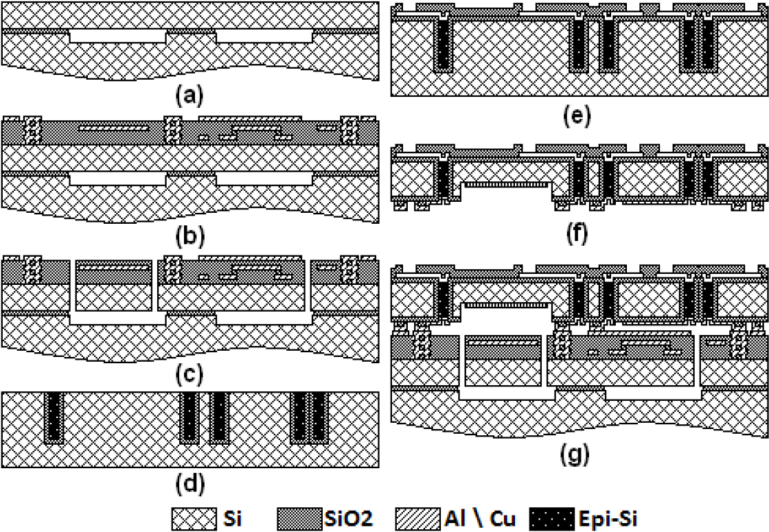
As you can see, the TSIs have walls of oxide; they’re then filled with highly doped n-type epitaxial silicon. Getters are placed in the vacuum side to help to maintain that vacuum after it’s in place.
They had to play a number of games to deal with stress issues. Large diaphragms tended to be bent by the vacuum during fabrication, so they added temporary supporting pillars (which were eventually removed). They then filled any remaining “sags” with oxide and planarized it all nice and flat.
There was also a stress issue caused by hysteresis in the temperature stress response to the 430-°C Al/Ge bonding temperature used when affixing the cap wafer. It affected the dielectric layers between the coils. They solved this by optimizing the order of layers in the dielectric stack, which involved films of SiO2 and SiN.
Other stress-reduction techniques included reducing sensor area, using circular structures, and placing trenches in the dielectric layers.
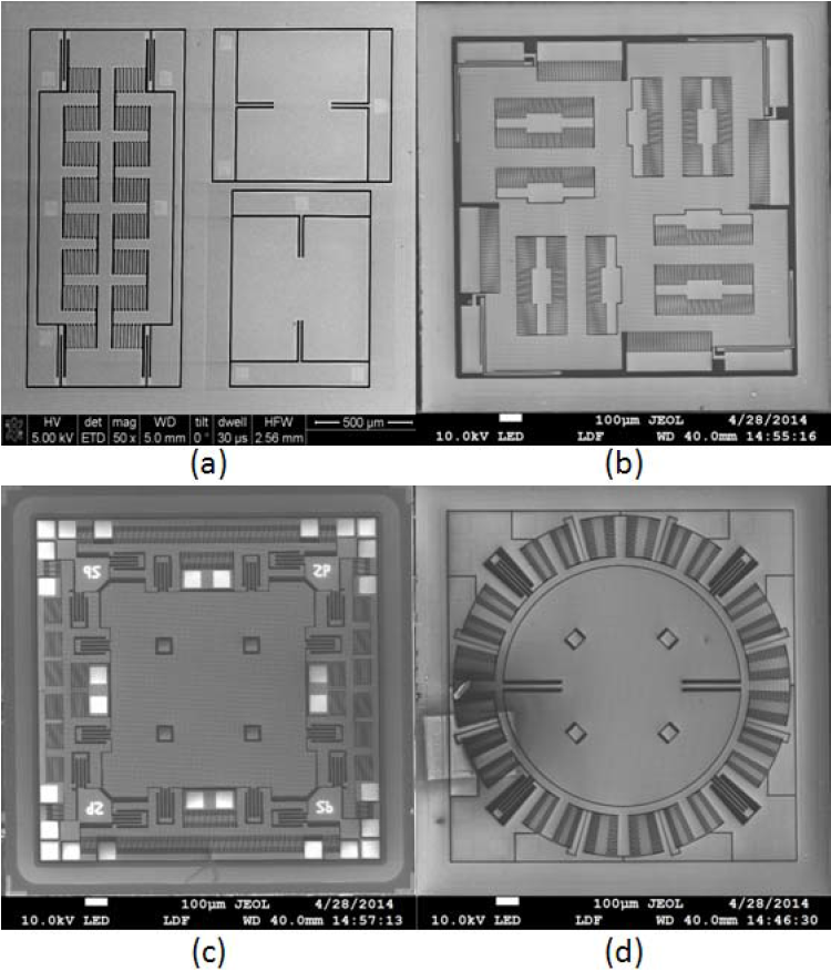
The image below shows (a) the magnetometer, (b) the accelerometer, (c) the z-axis gyro, and (d) the x/y-axis gyro.
The paper is, “A Monolithic 9 Degree of Freedom (DOF) Capacitive Inertial MEMS Platform,” Ilker E. Ocak et al, Institute of Microelectronics, A*STAR (Agency for Science, Technology and Research), Singapore
Phononic Crystals for RF MEMS (22.5)
We turn next to RF MEMS. My first impression was that this is one of many “here are 20 things we did to make improvements to the following 5 figures of merit” papers. But it has a little something extra in there.
As dimensions shrink, it becomes harder to manage the thermal and power requirements of an RF resonator. What this team did was to add “phononic crystals” (PnCs) to the mix. They built their PnC by drilling carefully placed holes in the AlN layer that was also used to fabricate the resonator.
As a reminder, phonons are pseudo-particles used to represent vibration behavior in crystals. So this is really an acoustic device, and they designed it with a bandgap (yes, PnCs have a bandgap!) centered at the main resonating mode frequency – meaning that those frequencies cannot pass through the PnC.
As a result, the vibrations from the resonator are transmitted (along with heat) up to the PnC. The PnC carries the heat away, but it reflects the vibrations back into the resonator. A really simplistic way of looking at this is that you’re containing energy that would otherwise have leaked away, improving the electromechanical coupling. (And, you would think, reducing the actuating power required…)
The bonus they got was that they were able to replace the “release windows” – those big holes through which etchant can flow to detach the bottom parts of the MEMS structures and free them up to move – with the PnCs (which still allow etchant flow and so do double-duty in the release phase). This means that they got the PnCs for a negligible change in die size, as you can see from the photo below.
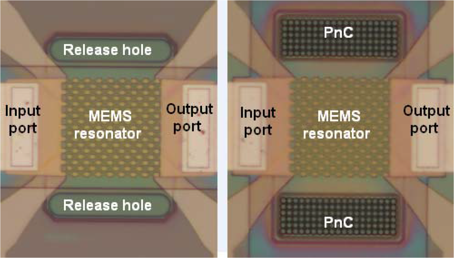
The paper is, “Integration of RF MEMS resonators and phononic crystals for high frequency applications with frequency-selective heat management and efficient power handling,” Humberto Campanella et al, Institute of Microelectronics, A*STAR (Agency for Science, Technology and Research), Singapore, and Department of Electrical and Computer Engineering, National University of Singapore.
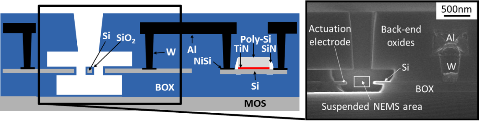
NEMS and CMOS (22.1)
We now descend into the realms of NEMS. It’s too easy to think of NEMS as just smaller versions of MEMS devices, but that’s not accurate, according to this paper. NEMS doesn’t necessarily replace MEMS applications (although, as we’ll see, the one they showed is something we’ve looked at in a MEMS context); they see it as opening up new applications.
This paper is more of a high-level treatment of NEMS/CMOS integration issues and approaches, with some sample circuits and devices. Much of it alludes to future work leveraging these concepts. They define NEMS as mechanical structures where 2 out of the 3 dimensions are smaller than 1 micron. So, for instance, you might have a long beam – the length is longer than 1 µm while the cross-sectional dimensions are below that limit.
In this realm, elements are more exquisitely sensitive (both to useful and useless stimuli), with very fast response.
They note that, while MEMS and CMOS together on a single die was a goal for a while in the past, that’s largely petered out; MEMS and ASIC dice remain stubbornly separate (even in cases like InvenSense, where the two dice are bonded together). It’s simply not cost effective to do, and the benefits don’t really play out at the MEMS level.
In addition, with MEMS devices, the off-chip readout circuitry noise dominates. But at the NEMS level, when integrated with the circuitry, the NEMS signal-to-noise ratio (SNR) becomes the dominant factor. In fact, they use SBR – signal-to-background ratio – as a critical metric.
One application they discussed was an analyte detector – yes, we’ve talked about those before, so they have a MEMS analog. In this case, we have a simple single beam collocated with its circuitry.
For practical commercial devices, the sensitivity means that you’re probably going to need multiple sensors to extract some statistical meaning. Single elements will be replaced by arrays of elements – and yet you’ll need to be able to address those elements individually for testing and in case low-granularity data is desired. That makes on-chip circuitry much more valuable.
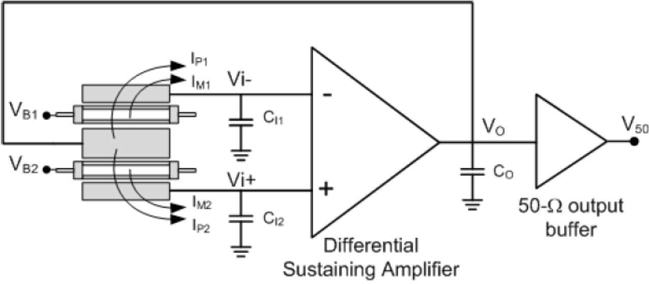
By integrating CMOS and NEMS, each “pixel” in such an array can be its own self-oscillator; they mentioned a couple of examples from other works, including the one below.
They also looked forward to future possible new transduction methods as the limits of capacitive sensing are reached; I’ll leave those details in the original paper for the curious reader. There’s much more there than I’ve elected to extract.
That paper is, “Nanosystems monolithically integrated with CMOS: emerging applications and technologies,” J. Arcamone et al, Univ. Grenoble Alpes; CEA, Leti, France.
Poly-Si nanowires (22.4)
The next paper studied nanowires in a mass detection device. This amounts to what we’ve talked about for analyte detection (clearly a popular application): having an element that can tell when some mass has landed on it. The gold standard – or perhaps better to say silicon standard – for this has been to use crystalline silicon for the nanowires used to detect and magnify stresses (as Leti discussed a couple of years ago). This paper characterizes a poly-si alternative – attractive because it’s cheaper to manufacture.
Just to get a sense of the amount of mass we’re talking about here (if getting a sense is even possible),with crystalline silicon nanowires, they can detect down to 1 zg. Yeah, that’s “zeptogram.” And yeah, I needed to go look that up as well to remind myself where it stands in the unit-prefix pantheon: it’s 10-21 grams, below atto- and femto- (and pico- and nano-).
They delve deeply into the materials details; I’ll skip to the punch line in that they were able to get good quality with poly-Si nanowires (Q of 130 in air; 3900 in vacuum) and the ability to resolve masses down to the 100 zg level.
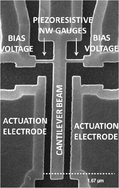
The paper is, “High performance polysilicon nanowire NEMS for CMOS embedded nanosensors,” I. Ouerghi et al, CEA, Leti, France.
Nano-Drumheads (8.1)
We round out the discussion with investigation of 2D materials for building NEMS membranes (nembranes?). The authors of this paper note that much NEMS work has involved 1D elements: tubes, nanowires, beams, and cantilevers built out of silicon, SiN, SiC, diamond, carbon nanotubes, and III-V materials. The paper claims to be a first attempt to investigate the properties of 2D materials on 2D structures.
We’ve looked briefly at such materials as MoS2 before, but in the context of futuristic transistors. In this case, they’re laying the materials down, layer by layer, to build up a structure. They define the “membrane regime” to be less than 10 layers thick; above that, you’re in the “disk regime.”
The benefits of 2D materials are listed as having low mass for a given area, high elastic modulus, strength, and flexibility. Undriven, MoS2 even has an intrinsic Brownian resonance. Yeah, I know… if we get much smaller, we’re going to have quantum-level structures popping into and out of existence…
In addition to exploring the properties of MoS2 resonators, they built an electrically tunable RF resonator along with variants. At this level, it’s hard to discuss the figures of merit without delving into a lot of detail; suffice it to say that they saw significant promise.
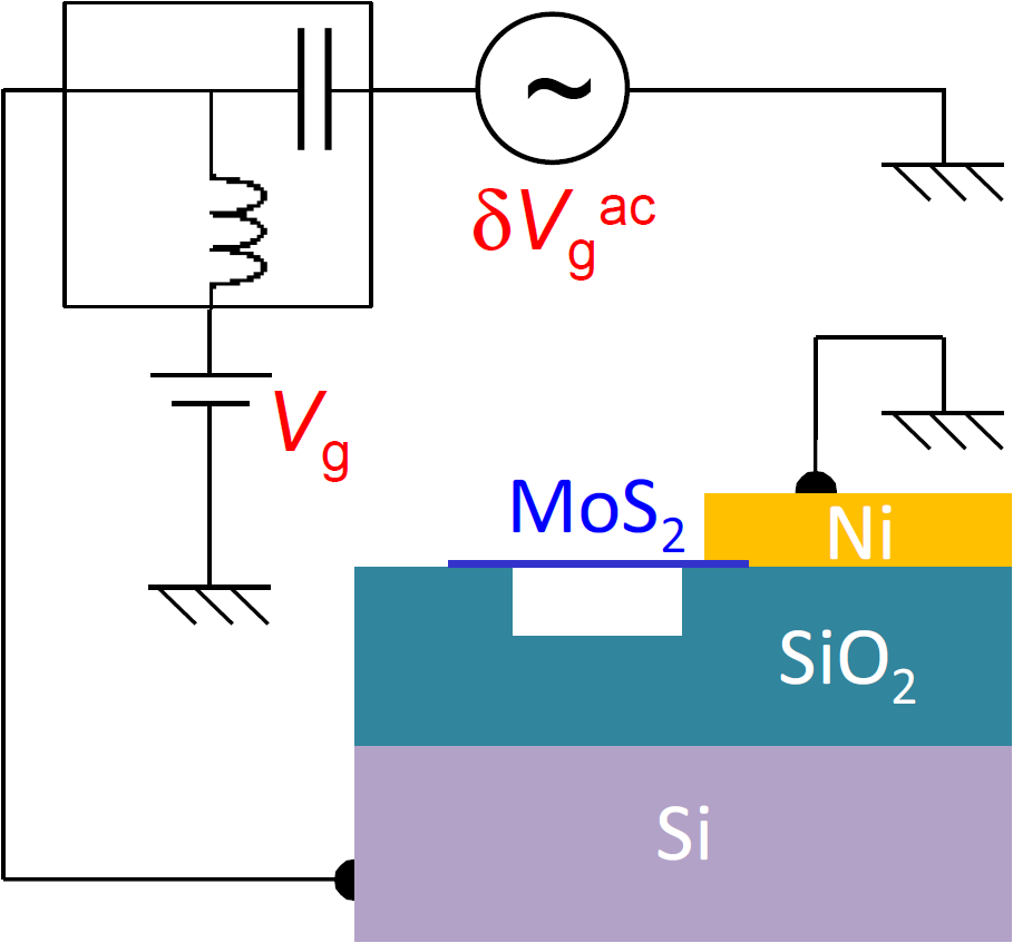
Not intuitive, however, is the fact that they see non-idealities in the MoS2 as paving the way to more features, allowing designers to play with frequencies, modes, frequency spacing, and mode shapes and splitting in a way that isn’t possible with ideal MoS2.
The paper is, “Two-Dimensional Nanoelectromechanical Systems (2D NEMS) via Atomically-Thin Semiconducting Crystals Vibrating at Radio Frequencies,” Philip X.-L. Feng et al, Case Western Reserve University and Pennsylvania State University.
See you next December.
All images courtesy IEDM.
* That said, two weeks ago, both SPIE Advanced Litho and ISSCC happened, the latter of which decided for some reason to move from their traditional non-conflicting date to clobber SPIE Litho… So I allocated one day for ISSCC – and, being sick that day, I decided not to infect the engineering community. So for the first time since I’ve been doing this, I won’t have anything to report from ISSCC…


Do any of these MEMS/NEMS ideas look useful to you?