


One of today’s biggest Silicon Valley gripes is the evaporation of venture capital (VC) funding for chip startups. Since the dotcom bust, consumer application-driven silicon innovation has been reduced to a relentless chase after Moore’s Law – improving power, cost and speed for incremental multimedia and wireless enhancements in a race down the consumer product generational roadmap to Inventiveness Oblivion.
With 40+ years combined founding and joining startups and working for giant chip and systems companies, the authors have seen Valley booms and “game changer” technologies come and go. Now, though, industry veterans feel Silicon Valley isn’t re-evolving, but dying.
Revolutionary, disruptive IC technology invention has shrunk dramatically. Complaints amongst Valley veterans are spat out thru clenched teeth over beers in old watering holes as VC funds now flow towards Web 2.0 ventures coding new search engines, social media websites, Cloud and smartphone apps. Funding cloud ventures has benefits – IT outsourcing to software/network/infrastructure-as-a-service (SaaS/NaaS/IaaS) has breathed some life into networking and storage chipmakers, even spurring SERDES and memory innovation. But old Valley hands see today’s Web 2.0 funding not as investing in the technology firms that Wall Street and mainstream media think they are, but actually advertising and media ventures exploiting a new channel.
The negative effects on Silicon Valley are despairingly evident. Acres of empty South Bay office space resemble Wild West ghost towns. Companies die or are absorbed in mergers. Where there were 15 chipmakers per block, there’s only 2 or 3. Along with consolidation comes suffocating bureaucracy, as big company procedures and policies crush any spirit of entrepreneurship and innovation in cube farms in favor of security, predictability and the illusion of management control. Lack of fresh thinking concurrently saps long-term strength from larger organizations as consumer BU’s endlessly squeeze costs, eroding operational effectiveness and eventually getting sold or disbanded. This has driven bigger chipmakers to find small, neglected niches with poor growth potential, low pricing and poor margins that they can dominate, worsening segment financials and creating barriers to entry. Some Valley companies are ahead of others down this path of deliberately pursuing third tier status, preferring the stability and security of their stagnant pond over the challenges in the ocean with the big fish.
VC’s aren’t to blame, however. Sand Hill Road strove to be savvy technology incubators, but their deep-pocketed investors forced them to be bankers specialized in risky technology bets. This penchant for risk taking – laudable in spirit – had an unenviable track record, with 1 startup in 10 breaking even, and 1 in 20 becoming viable. Who can blame them for rejecting today’s chip ventures, where it’s normal for a startup to go thru 4 rounds, spending $100M+ and still be struggling? With such terrible ROI, VC’s logically prefer giving $500k – $1M to a posse of coders who build a smartphone app that returns 10x in 6 months.
So: is Silicon Valley doomed? Despite a concentration of expertise and intellect unparalleled in the history of civilization, fresh talent locally infused from two world-renowned universities, and year-round weather between early and late spring, are the few remaining companies in what was once the world capitol of high technology inexorably headed towards also-ran status? Has the spirit of Invention permanently fled to the lands between Shenzhen and Beijing with (currently) lower personnel costs and colossal government funding?
Capital Lite
The Global Semiconductor Alliance (GSA) is trying to reignite chip startup activity thru a coalition replacing VC sponsorship with established chipmakers, services firms and manufacturers.
The GSA’s Capital Lite Working Group is gathering a $100M Angel fund. Releasing funds would require startup sponsorship from a contributing chip firm that would need to support the startup with a “toolkit” provided directly or pooled by fund contributors. Per-startup fund disbursements would not exceed $10M.
The toolkit could take several forms. The premise is that the sponsor has generic IP, channel, and marketing, sales and engineering that could be conditionally provided – i.e., generic IP would be swapped for equity, variable IP licensing and royalty terms based on trigger events, and co-development would reduce funding requirements.
Though praiseworthy, the proposal is problematic:
- It’s balance sheet-oriented – financial controls are the only consideration.
- The sponsor’s IP isn’t a ”sunk cost.” Creating embeddable, transferrable IP – with hardened or synthesizable cores, EDA files and scripts, verification suites, SDK and SW stack, all portable and documented – takes expertise, time and resources. There are support and maintenance costs beyond those already carried by the sponsor, since the IP portfolio effectively becomes a product line.
- Even strong Valley chipmakers are experiencing margin squeeze from lower-cost global competitors – preventing recruitment to support customer issues, product enhancements, demand generation, and new product development. Combined with a weak business climate, how can firms offer tools, IP and resources to a startup?
- Since chipmakers, service providers and manufacturers are expected to be Angel fund contributors and also must provide startups further resources to access the fund, the initiative essentially transfers VC financial burdens to the chip industry. However, service providers dedicate personnel to revenue activities, and cannot depend on payment promises from risky ventures; furthermore, their cash flows can’t support Angel fund contributions. Manufacturing chain impact on startup costs (besides masks) is minimal, and their margins are worse than the service providers. Thus the GSA approach is restricted to deep-pocketed chipmakers.
Big chipmakers sometimes finance their own ventures. Valley giants have sponsored “rifle shot” startups – Cisco and Broadcom are two well-known examples. However, disruptive invention costs – and risks – are born solely by the sponsor. Even with a resolute executive management team in it for the long haul (a rare occurrence), there will be organizational friction – departments will be reluctant to redeploy safely committed budget and resources to efforts with doubtful outcomes.
Though the GSA proposal is applicable to the strongest Valley firms, it doesn’t provide a framework for the industry as a whole to broadly revitalize the chip startup environment, where many potentially disruptive technologies can be pursued and survivors go on to have wide impact. It also reflects a financier’s mindset of managing problems thru balance sheets and income statements to make the final decision. Since most new inventions fail to meet early expectations, this bureaucratic approach is unsuited for high tech.
The GSA’s proposal doesn’t recognize that the traditional chip startup model is obsolete. What’s required is a fundamental rethink of the process of building a startup, the essentials of product development, getting it right the first time, and ensuring your product succeeds with the greatest number of customers at volume ramp.
Ironically, the solution can be found deep within the belly of the beast that the Silicon Valley old guard loathes so viscerally – the maelstrom of Web 2.0 companies trying to replicate the success of Facebook, Groupon, eBay and Google. Valley veterans make a great mistake by turning a cold shoulder to it, for hidden within is a tiny group of entrepreneurs who genuinely share the spirit of Bill Hewlett and Dave Packard – Silicon Valley pioneers who labored in a Palo Alto garage in 1939 with $500 of their own cash as seed money and a broken voltmeter wrapped in bailing wire.
Lean Startup
Eric Ries is one of those entrepreneurial minds. His “Lean Startup” concept uses Rapid Hypothesis Testing of a new product concept on a broad customer base and frequent product reengineering to develop a minimum viable product that meets 80% of the broader market requirements. Employed properly, this approach cuts cost by eliminating waste and over-engineering and jumpstarts market acceptance.
The Lean Startup approach is a leap forward from Geoffrey Moore’s groundbreaking “Inside the Tornado” and “Crossing the Chasm.” Whereas Moore’s approach targets early adopters as the first revenue drivers and then transitions products to the full requirements of early and late-majority mainstream users, the Lean Startup method bypasses early adopters’ non-standard requirements. Product, application and market assumptions are tested frequently against the wider market, so the offering gains mainstream acceptance much faster, reducing development time and accelerating and magnifying production ramp.
However, Ries developed this approach in the Web 2.0 environment, characterized by very fluid, short product life cycle and low investment, where cost is restricted to workstations, servers, some SW developers, and an office and furniture. How can this Lean Startup concept for low/medium complexity SW products work for astonishingly complex chip or system-on-a-chip (SoC) development, if at all?
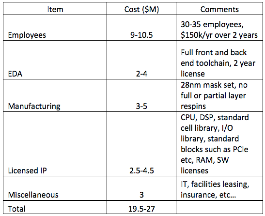
Table 1 estimates costs for a new chip venture. These are ideal case numbers, with zero showstopper technical problems designing or debugging, right-first-time analog and mixed-signal hardware, and the first-product marketplace success. (Disclaimer: the authors do not believe in Santa Claus, Magic Fairy Dust or Unicorns. Also – numbers are estimates, your mileage may vary.)
Table 1 – Conventional Chip Startup Financials
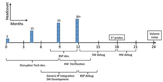
A timeline is given in Figure 1. The team begins from a base of HW engineers, recruits more HW and SW expertise over 9 months, peaking with manufacturing (operations, test and product engineering), business development (sales and marketing) and administrative overhead. Volume ramp includes final board support package (BSP) and SW distribution.
Figure 1
The startup is self-contained, with all talent, tools and equipment brought in-house. However, this model began failing 10 years ago with 0.13um, when multimillion gate designs became routine. Integrating CPU’s and DSP’s lead to SW integration and the birth of the SoC. Rising complexity increased development cost (primarily masks and engineering teams) and greatly magnified both the risk of failure and the financial consequences. Any timeline interruption indicates major failure of either product development or market adoption, and thus quickly doubles total cost. In fact, everyone reading this can name 3-4 chip startups that began with great promise that are now past their D round and still unprofitable.
Consequently, SoC’s are built by established companies that entered these markets years ago thru acquisitions. With the parent company’s size buffering resource or cost issues and the acquisition’s existing revenue stream, large chip firms have increased barriers to entry for newcomers with revolutionary ideas and further worsened the risk/reward ratio for VC’s.
Yet, as with all things in life, even carefully laid plans have unintended consequences. New technologies eventually become standard; incremental optimizations and value-adding enhancements result in quickly diminishing ROI, reducing competition to cost. This was never Silicon Valley’s strength, and technology centers with strong manufacturing – Japan, Taiwan, and increasingly Korea and China – are taking the consumer electronics business. Even the mobility-driven increase of infrastructure demand and its modest stimulus to startup-based innovation is proving insufficient to stem the rising tide of APAC firms in the networking segment as well. Thus, many of the remaining Valley firms, having lost access to breakthrough technology, find their consumer business units (BU’s) withering on the vine, and their networking BU’s losing ground.
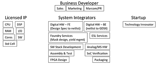
Using the Lean Startup model avoids the classic model’s financial, technology and market risks by literally breaking up the monolithic startup. Figure 2 shows a “distributed startup” ecosystem for developing disruptive SoC technology and bringing it to market faster with first time success.
Figure 2
The last decade has produced a plethora of unintended consequences. The relentless drive to cost-reduce consumer electronics and the now 4-year-old recession led to continual layoffs in chip firms. In order for this released talent pool to make ends meet, many have created partnerships and bootstrapped ventures with former colleagues also at loose ends.
This is analogous to the British electronics sector of the early 90’s. After the Berlin Wall fell, thousands of engineers laid off from British defense and aerospace companies formed groups to turn their abilities and experience into a source of income. Teams would form, dissolve, and re-form with different members until something”stuck.” Helped by a few companies, interested Cambridge professors and grad students, by the late 90’s Britain had the most innovative Wireless electronics industry on the planet.
Silicon Valley’s talent pool mirrors that of Britain 20 years ago. They’ve seen demand for their talents as contractors from chipmakers increasingly outsourcing on a project basis. Accordingly, small firms have risen with highly focused expertise offered for “lease.” This is a kind of “licensable intellectual property.” The advantages to firms large and small echo those of conventional HW or SW IP licensing – a licensor doesn’t bear all ownership expenses, but ”rents” the IP, sharing costs with other clients of the IP provider.
Startups can thus virtualize most plant and personnel. The central element – the technology inventor – is the only one needing direct financing.
Let’s examine the ecosystem’s segments. For “paraphernalia” IP, there are many vendors for standard functions (PCIe, USB 3.0, peripherals, etc…) Some have multiple components – for instance, Dolphin Technology and its high performance SRAM compilers, standard cell and I/O libraries. Few offer more than 70% of the selection, such as Synopsys and ARM. Rather than developing IP in-house, a startup shares the IP ownership cost with 10-30 other companies and gets the core or code delivered electronically, along with tool files, documentation and support.
The same applies to system integrators. Individual suppliers can be found for each category. Fabless ASIC houses capture several, such as back-end digital HW engineering and manufacturing from GDSII thru assembly, test and production. Few can do 90% or more. But with larger firms having liquidated entire SW and HW SoC groups, some people have found each other and formed their own multi-skilled teams.
The hardest segment to manage is the business developer. Finding contractors to code HTML for a website is easy. Finding a marketing consultancy that has a verifiable track record in digital and general marketing services isn’t. The rarest are business developers that offer a large company’s marketing/sales/field applications department on a “rental” basis. Such consultancies possess deep experience marketing and selling complex products to engineering teams, enticing interest while demonstrating technical credibility (theirs and the technology’s) so that engineers will eagerly use the new product and not fear they’re investing time, energy, intellect, reputation and job security in an Edsel. Managing an engineer’s instinctive attraction to technical novelty while insisting that it must also be a robust, safe solution – the “Macho Nerd” paradox – takes a rare combination of business and technical acumen.
Applying this ecosystem to the Lean Startup method is critical. The key is to maximize parallelization of HW and SW development while simultaneously supporting rapid hypothesis testing with many customers. Testing frequency is vital, as over-engineering, feature-creep and non-standard specialization must be avoided, leapfrogging early adopters and gaining immediate mainstream acceptance for a “hockey stick” production ramp.
Figure 3
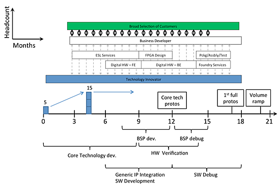
The technology inventor – the core talent developing the differentiating, value-adding, disruptive HW/SW technology – plateaus at 15 people early. QA, verification, or any other engineers not designing the disruptive technology are outsourced.
Business development is involved early and continuously. Working closely with the tech inventor, they iteratively and broadly verify customer appeal. Hypothesis testing failures are resolved by the tech inventor directly or thru the system integrator.
Prototyping begins early with electronic system-level (ESL) modeling, updated continually as the disruptive IP advances thru development and “Paraphernalia” IP becomes available. FPGAs bridge the gap between ESL modeling and full silicon, with shuttle-produced disruptive IP on an FPGA board emulating missing HW, supporting “paraphernalia” IP and running at some fractional target clock speed. Final BSP and SW distribution are available concurrently with first silicon, allowing customers and the tech innovator to confirm that the minimum viable product has indeed been reached.
Ramp from first silicon to volume is swift, because the first prototypes are the minimum viable product. All that’s necessary is final customer ratification. 3-4 months are shaved off development thru hypothesis testing, eliminating unnecessary development.
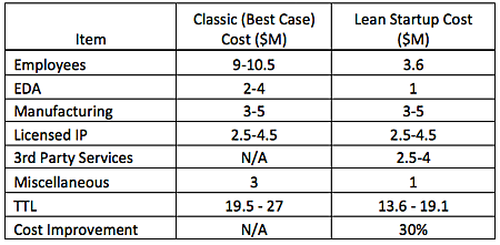
Besides accelerating time to market and revenue, the Lean Startup method saves 30% by “renting” services only when needed, hiring fewer people, and reducing EDA licensing costs (since system integrators carry those for their own operations.) Should the idealized classical model fail to deliver a runaway hit product on its first release, Lean Startup cost savings rise exponentially to 300% or more.
Table 2 – Lean Startup Financials
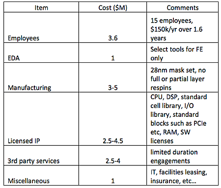
Table 3 – Classic (Best Case) vs Lean Startup Financial Models
There are many other ways to reduce cost, shorten development time and increase success – including a new role for VC’s, verification and ESL advances, startup/ecosystem/chipmaker partnership methods, and future directions for possible disruptive inventions. These and other ideas can be further elaborated in the future.
In these dark days in Silicon Valley, the seeds of change await the will to use them. The Lean Chip Startup model provides a detailed framework for doing it.
Authors:
Peter Gasperini – VP of Business Development, Markonix LLC; previously President and GM of Iunika North America, with 22+ years of experience in Silicon Valley with ASIC, FPGA, embedded microprocessors and engineering services.
Qasim Shami – CEO and co-founder of Comira Solutions; previously, VP of SW development and architecture at Ikanos, with 15 years of leading engineering teams and organizations for SoC HW and SW development.
Contributors (abridged):
Amit Dhir – Director, PwC Advisory/Management Consulting; previously, VP of Vertical Markets at MIPS
Rakesh Patel – Consultant, Strategic Initiatives at Global Foundries; previously Sr. Director R&D IC Design at Altera
Suk Lee – Director, Design Infrastructure, Marketing Division, TSMC; previously, VP and GM, CBDU at Magma
Bob Caulk – VP of ASIC Design at TZYX; previously, Chief Architect at Metta Technology


These gentlemen have proposed a new way of spurring innovation in Silicon Valley. What do you think?
This is preposterous. American companies and workers are simply getting what they deserve. They’ve controlled technology against everyone else, it is now time for us to take back what belongs to us. Americans will work at mcdonalds and walmart and spend their money at NASCAR and buying the future complex mobile products and TV’s, set tops and gateways that WE will invent, because we are better educated and know what it really means to work hard.
That’s pretty unfair; you should try working at my company sometime…..
The authors make some interesting points, but there’s other things to consider – most everything is sw driven now, and the truth is that silicon valley hasn’t invented or innovated for a long time now. HW changes are optimizations today, and anything new doesn’t come from the valley anymore. It really looks like the days are gone where it’s the tech capitol.
Color me impressed! But I don’t know if
I’d let the venture capital people off the hook so fast. They’re supposed to be the experts at picking tech winners and losers, so there really is no excuse.
EDA tools and mask sets are where the costs really are. EDA should be able to do a lot to improve things. Masks, I don’t know, but it’s basic engineering to work on driving costs down. That’s where the focus needs to be.
The Lean Startup model seems reasonable, but I remain unconvinced Silicon Valley would be any better at executing this than other venues. The chief advantage the valley had for so long was the concentration of the world-wide talent, and in this era of globalization that talent is now diffused.
The other big problem for chip startups in general is fundamentally what problem are they attempting to solve and what is the value of their solution? The premise of their existence is based on the development of a disruptive technology, but at what cost? In other words, is it even possible for any model to work if “the juice just ain’t worth the squeeze”?
The problem it seems is we are still stuck on Moore’s law. AS long as we are on that road, expect no innovations from anybody. We need a radically different approach or methodology to spur innovations.
It’s absurd to believe (a) that Moore’s Law is a law rather than a prediction, (b) that even people who care about Moore’s Law let it prevent them innovating. Where are the Moore Police? Right.
Having worked for almost 3 decades at a few paces behind the leading edge, I’ve seen nothing but opportunity to create and innovate. Maybe the whole chip is nothing crazy, but there’s always something you can do better.
The problem for small semiconductor startups is that you can’t and won’t break large on your first design. There’s just no way. No major product rollout, no big orderly company full of ISO- this and TS-that, is going to hang the whole thing on some shoestring outfit that’s never demonstrated they can (and more importantly, will) deliver the goods on spec, on time, no surprises, no excuses. And the little guys can’t even manage the paper mountain getting the certs these big customers require, entails. The electronics industry that sits above semiconductors has become too rigid and choking.
I’m looking to start a semi house, without the VCs – they give you money, great, but they then want to make you run the business just like every other business is run, which will kill your differentiation and your key contributors’ enthusiasm in short order.