


My mission today is to inform you about a university course that is no longer offered and a master’s degree program that is not yet available. Intrigued? Read on…
To set the scene, first let me remind you that I originally hail from England. I started at Sheffield Polytechnic (now Sheffield Hallam University) in the summer of 1975. You can read more about how this all came to be in my column, There’s More Than One Way to Become an Engineer (Part 1).
At that time, the only computer we physically had in the engineering department building was a room-sized analog beast. We also had access to a ballroom-sized digital behemoth in a separate building, for which we were obliged to capture our programs (in FORTRAN) on decks of punched cards that we then hand-carried across the road to those who served the monster mainframe.
My course was in Control Engineering, which involved a core of mathematics coupled with mechanics, electrical and electronics, and hydraulics and fluidics. We spent a considerable amount of time studying control theory, primarily in the context of analog proportional-integral-derivative (PID) controllers. When it came to the digital side of controlling things, we were largely limited to bang-bang (on-off) control, mayhap involving a hint of hysteresis (if we were lucky).
With respect to raw electronics, we covered both the analog and digital sides of the divide; however, the latter was limited to combinatorial logic and simple sequential logic. Microprocessors and microcontrollers had not yet made their presence felt in the course curriculum.
Digital signal processing (DSP)? Don’t make me laugh. Although early-stage DSP did exist in the world, it wasn’t even mentioned in passing during my course. As a result, DSP is one of the (many) areas in which I lack expertise. By the time DSP became mainstream, I was too busy working my socks off to learn it to any decent depth (sad face).
Contrast this to my friend, Adam Taylor, who entered Sheffield Hallam University’s hallowed halls 20 years after your humble narrator (I pride myself on my humility). You can read more about Adam’s story in my column, There’s More Than One Way to Become an Engineer (Part 2). By the time Adam started in 1995, heavy-duty DSP was at the forefront of the course, alongside components like FPGAs, which were still 10 years in the future when I set a trepidatious toe across the institutional threshold.
Why am I waffling on about all this? Well, we are in much the same position today with respect to artificial intelligence (AI) and machine learning (ML) in the context of semiconductor engineering. Although early work on AI and ML kicked off in the late 1940s and early 1950s (the terms artificial intelligence and machine learning were coined in 1956 and 1959, respectively), it’s only relatively recently that these technologies have started to make their presence felt in the real world.
What do I mean by “relatively recently”? Well, Gartner, Inc. is a renowned American research and advisory firm specializing in information technology (IT) and related industries. In 1995, Gartner introduced the concept of the Hype Cycle, a model that describes the evolution of new technologies over time in terms of expectations and adoption. The Gartner Hype Cycle features five key phases as follows:
- Innovation Trigger: A breakthrough or concept generates interest. No usable products yet, but media and early adopters are excited.
- Peak of Inflated Expectations: High publicity leads to unrealistic expectations. Some success stories, but many failures. Hype is at its highest.
- Trough of Disillusionment: Reality sets in. Early implementations fail or disappoint. Interest wanes, and companies may abandon the technology.
- Slope of Enlightenment: Gradual improvement as practical uses emerge. Second-generation products appear. Realistic understanding grows.
- Plateau of Productivity: Technology matures and becomes mainstream. Adoption increases where it makes sense. Real, measurable benefits are seen.
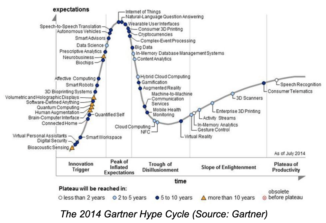
Consider the 2014 version of the Hype Cycle as illustrated below. You’re right; there’s no mention of AI or ML anywhere because these technologies simply had not yet impinged themselves on the public consciousness.
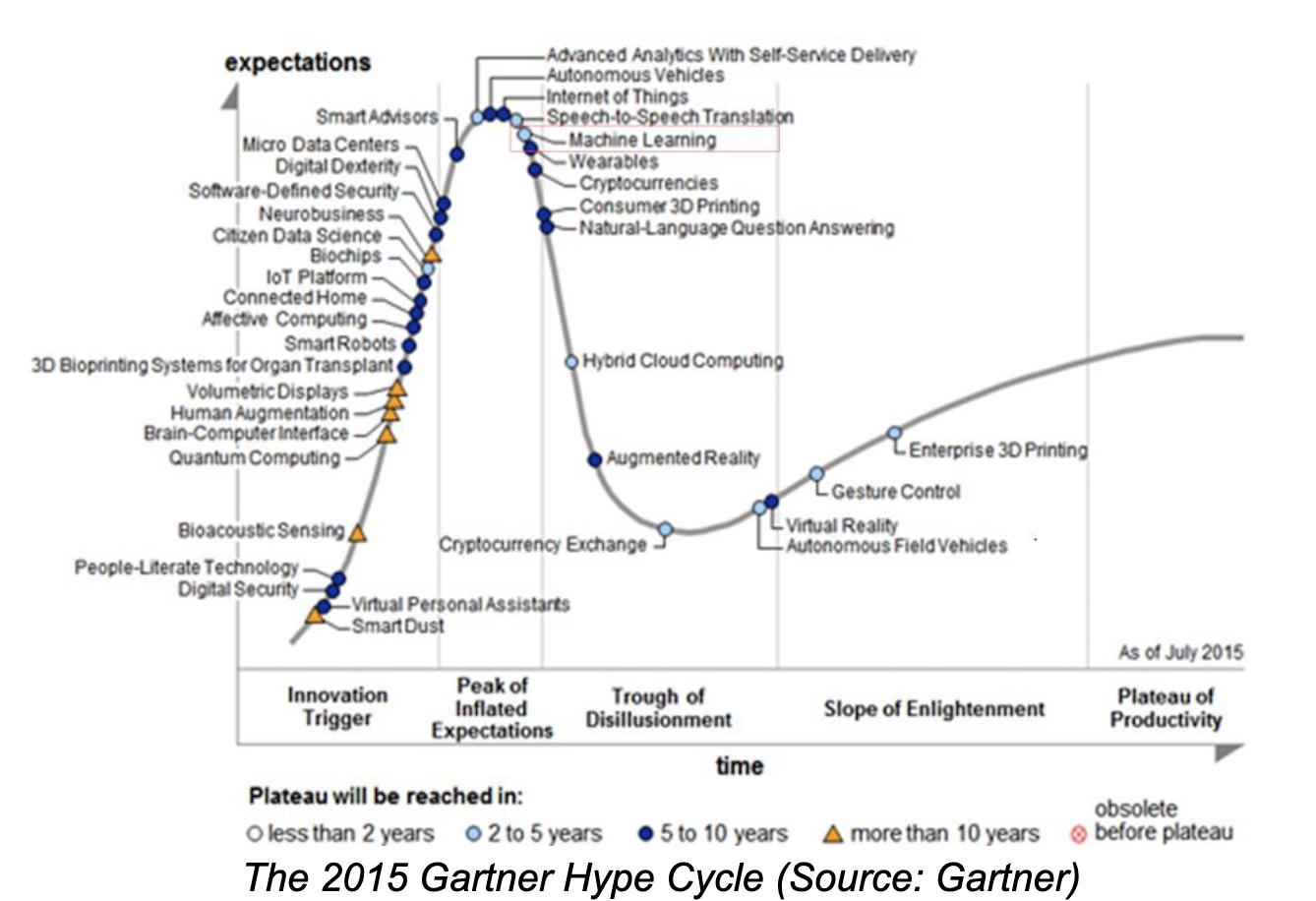
By comparison, consider the 2015 version of the chart depicted below. Good Golly Miss Molly! By this time, just one year later, machine learning (indicated by the red box) had already surmounted the Peak of Inflated Expectations!
On the one hand, 2015 seems like a lifetime away, but that’s only because things are moving so fast. In reality, 2015 is only ten years ago in the rearview mirror of life as I pen these words. It seems as though every time I blink these days, I discover yet another decade has passed me by.
Semiconductor fabs are complex beasts. There are thousands of steps in the semiconductor manufacturing process. Petabytes of raw data are collected, but the process of analyzing it is so complex that most of this data ends up being discarded. Few existing semiconductor engineers at the fabs possess in-depth expertise in AI/ML. Meanwhile, many of today’s students do learn AI/ML, but only at the “It’s a dog,” “It’s a cat,” or “It’s a duck” level. They don’t learn how to work with the petabytes of data associated with real-world semiconductor manufacturing.
If things don’t change, it’s anticipated that 67,000 semiconductor positions will go unfilled by 2030 (39% will require post-secondary certificates or two-year degrees, 35% will require four-year engineering or computer science degrees, and 26% will require a master’s or doctoral degree).
CHIPS Act(s) are being enacted around the world, bringing advanced semiconductor manufacturing into new regions. Additionally, these newly announced fabs are designed to be general-purpose foundries, handling a wide range of chips, as opposed to Integrated Device Manufacturers (IDMs) that specialize in building just a few chip designs. Meanwhile, graduating engineers have very little training on integrated circuit (IC) manufacturing data in the first place.
All of this leaves us in a bit of a pickle (I hope I’m not being too technical).
Happily, you can turn that frown upside down into a smile, because I am the bearer of good news. It starts with a company called PDF Solutions, which was founded in 1991 by two recent PhD graduates of Carnegie Mellon University, John Kibarian and Kimon Michaels, who had the vision to combine software, hardware, IP, and services to solve the aforementioned challenges.
Over the years, the guys and gals at PDF Solutions have invented innovative methods and tools to generate, collect, and analyze data, thereby reducing the total cost of IC design and manufacturing, accelerating time to market, and enhancing overall product quality and reliability. As a result, PDF Solutions is now an invaluable partner to more than 130 semiconductor companies, and its offerings are critical for Fortune 500 companies, including major foundries, fabless design houses, IDMs, and outsourced semiconductor assembly and test (OSAT) providers.
Headquartered in Santa Clara, California, PDF Solutions has extensive operations across North America, Europe, and Asia. In a crunchy nutshell, the chaps and chapesses at PDF Solutions specialize in transforming raw semiconductor manufacturing and test data into actionable foresight, enabling their clients to anticipate and address challenges before they escalate.
Recently, I got to chat with Andrzej Strojwas, Ph.D (Chief Technology Officer, PDF Solutions, and former Keithley Professor of Electrical and Computer Engineering, Carnegie Mellon University), Rishi Bamb (Data Science and Analytics Solution Prototype Engineer, PDF Solutions), Anya Jasthi (ML Applications Engineer, PDF Solutions), and Christophe Begue (VP of Corporate Strategic Marketing, PDF Solutions).
They explained how PDF’s ambition is to contribute to the scaling of available analytical skills for semiconductor manufacturing in the U.S. This is a multi-year, multi-person, multi-organization plan.
PDF began by collaborating with Carnegie Mellon University (CMU) to develop an initial project-oriented course to teach students AI/ML in the context of semiconductor manufacturing. As part of this effort, PDF created an original dataset (based on obfuscated real-world fab data) and provided analytics tools, a cloud-based environment, and instructional support.
The resulting course was highly popular, attracting more than twice as many applicants as there were available spots. Andrzej taught the course in the Fall of 2023 and again in the Spring of 2025. However, because many of the students lacked a strong background in semiconductor technology, it became apparent that a standalone course was insufficient. As a result, CMU decided to discontinue the course in its current form and instead have the Electrical and Computer Engineering (ECE) and Materials Science and Engineering (MSE) departments develop a comprehensive master’s program in Semiconductor Engineering.
PDF and CMU—working alongside semiconductor fabs and other academic institutions—are now collaborating on the curriculum for this new degree (the original course will become a core component of the expanded program).
It’s hoped that the new course will commence in the fall of 2026. In the meantime, many semiconductor companies have their own training programs to bring new employees up to speed on semiconductor manufacturing; however, these programs do not address AI and ML. To address this shortfall, the original course is being repurposed to address this in-house corporate training need.
In many ways, we’re witnessing history repeat itself. In the same way that DSP and FPGAs transformed electronics engineering education a generation ago, AI and ML are now reshaping what it means to be a semiconductor engineer. The collaboration between PDF Solutions and CMU represents a forward-thinking response to this shift, combining academic rigor with real-world data and industrial relevance.
As the semiconductor industry continues to evolve at breakneck speed, initiatives like these will be essential to ensure the next generation of engineers is equipped not just to keep up but to lead the way. It almost makes me want to be a student again… almost.
What say you? Do you, like me, hail from the days of yore, or are you relatively new to the engineering party? Either way, do you have any thoughts you’d care to share on anything you’ve read here?

