

When conversations turn to semiconductor foundries, they typically begin with leading-edge process nodes and the race toward ever-smaller geometries. However, although nanometer bragging rights dominate headlines, something quieter—and arguably more consequential—is unfolding elsewhere in the industry.
The reason for my newfound perspective is that I was just chatting with James Prior, who is a Marketing Executive at MIPS. James explained that a new class of computing is emerging outside the data center. Robots, drones, autonomous vehicles, intelligent infrastructure, and safety-critical industrial systems must sense, decide, and act in the real world, usually in milliseconds, often with strict power limits, and frequently with lifecycles measured in decades rather than years. This domain, increasingly described as “Physical AI,” is forcing a rethink of how silicon itself is conceived, designed, and manufactured.
Recent moves by GlobalFoundries (GF), its acquisition of MIPS in 2025, and its recently announced acquisition of Synopsys’ ARC processor IP portfolio in 2026, suggest that this rethink is no longer theoretical. Instead, it is coalescing into a vertically integrated effort to deliver custom physical AI silicon at foundry scale.
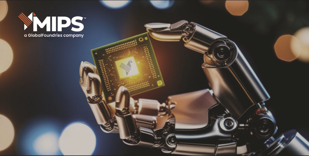
GF and MIPS are delivering physical AI at foundry scale (Source: MIPS)
GlobalFoundries has deliberately chosen to make physical AI a primary growth vector. Rather than competing solely in the shrinking-node arms race, GF is assembling the ingredients required to build complete compute platforms for autonomous, real-world systems. These ingredients include MIPS, bringing RISC-V processor IP, AI acceleration, software tools, and a storied embedded-system heritage; ARC processor IP, adding configurable embedded CPUs, DSPs, NPUs, and an established customer base; and GF’s own manufacturing, packaging, and custom-silicon capabilities, enabling deployment at an industrial scale.
Together, these elements create a unified pathway from architecture and software through fabrication and test, aimed squarely at accelerating physical AI adoption across transportation, robotics, industrial automation, and embedded infrastructure. In other words, this is not simply about selling wafers; it’s about delivering system-level silicon solutions.
Both MIPS and ARC share a deep RISC heritage, yet both ultimately moved toward RISC-V. The reason is less ideological than practical. Owning a proprietary instruction set means owning compilers, tools, ecosystem support, and long-term maintenance. By contrast, RISC-V distributes that burden across thousands of participating companies, while still allowing architectural differentiation in performance, efficiency, threading, and configurability.
When it comes to physical AI—where diversity of workloads is the rule rather than the exception—this flexibility is critical. There is no single processor that fits everything from tiny motor controllers to distributed robotic perception systems. Instead, physical AI demands scalable compute spanning low, mid, and high tiers, all interoperating within a common architectural framework. RISC-V provides the shared foundation, while customization provides the differentiation.
For decades, semiconductor IP followed a familiar pattern: “Here’s a processor core. Integrate it. Tape out. Hope for the best.” That ‘hardware-first’ model is rapidly breaking down under the weight of AI-driven system complexity. MIPS’ response is what it calls a ‘software-first’ methodology, enabled by its Atlas Explorer virtual platform, which allows customers to run real workloads on fully simulated processor models before RTL, FPGA prototypes, or silicon exist.
This shift-left capability enables two crucial insights: “Is the architecture right for the workload?” And “What hardware changes would improve efficiency or performance?” Developers can explore cache hierarchies, threading models, clustering strategies, and even architectural extensions, long before committing to the enormous cost of tape-out. The implication is that silicon is no longer the starting point; workload is.
Marketing phrases come and go (as I know to my cost), but in this case, the underlying concept is sound. A hardware-first design begins with fixed silicon boundaries and asks software to adapt. A software-first design begins with the intended workload and asks: What architecture best supports it? What configurability is required? And how must the silicon evolve over decades of deployment? This last question matters enormously in physical AI. Datacenter AI lifecycles may span only a handful of years, but industrial and automotive systems routinely demand multi-decade operational support. This means software-first thinking becomes less about convenience and more about long-term survivability.
At the center of this strategy sits the MIPS S8200 software-first RISC-V neural processing unit (NPU), designed to run modern multimodal AI, including transformer-class and agentic language models, directly on embedded and autonomous edge platforms. Rather than targeting cloud-scale throughput, the focus is on real-time inference, high efficiency, low power, and deterministic response for mission-critical systems.
Physical AI differs fundamentally from perception-only or cloud-hosted intelligence. To qualify, a system must interpret its environment, make autonomous decisions, and execute actions locally. Anything less is merely observation. This shift enables intriguing possibilities, such as privacy-preserving home intelligence that remembers events without storing video, predictive safety systems that intervene before failures occur, and autonomous industrial machines operating without continuous cloud connectivity. All share the common requirement of efficient, deterministic intelligence at the edge. And this, in turn, requires silicon built specifically for the physical world.
Real-world autonomy demands a different class of silicon: efficient, deterministic, customizable, and manufacturable at scale. GlobalFoundries, MIPS, and ARC are betting that the future of AI won’t be confined to hyperscale data centers, but will increasingly inhabit the machines that perceive, decide, and act all around us.
This is where things took a rather interesting turn, because James and I drifted into the topic of chiplets and multi-die systems (as you do). Just this week, as I pen these words, MIPS presented two papers at Chiplet Summit 2026: one on safety-critical physical-AI applications using RISC-V and the other on how software-first design enables earlier insights for smarter designs, reducing risk and decreasing time-to-market.
James noted that, from an IP perspective, “…the difference between a chip and a chiplet isn’t a whole lot… in fact, chiplets are easier because interfaces are more standardized and they fit into a bigger system.”
I’m afraid that this topic is a bit of a hobbyhorse of mine. We are still in the early days of chiplet-based design, but the long-term goal is to be able to mix-and-match hard chiplet IP from multiple vendors, then mount them on a silicon interposer and present the result as a single package. “But who will do the mounting and packaging?” I asked.
This was the point when James raised a quizzical eyebrow (I like to think it was amused rather than sardonic) as he pointed out that GF (and its OSAT partners) can package chiplets, assemble multi-die systems, and test and ship finished devices, all as part of the “foundry-scale” value proposition.
From MIPS’s perspective, the distinction between a monolithic chip and a chiplet is largely one of packaging and integration. Their processor IP can live in either domain, while GlobalFoundries’ manufacturing, advanced packaging, and partner ecosystem extend the pathway all the way to multi-chiplet production—an approach that is still evolving but is clearly central to the physical AI vision.
James hastened to add that full multi-chiplet modeling and the network-on-chip (NoC) simulation of multi-die systems are not yet fully realized, and that this is a vision that will unfold over the coming years, but that MIPS is clearly building toward chiplet-native physical AI platforms.
We are still in the “early innings” of physical AI (I fear my cricketing heritage is shining through). The terminology is evolving, architectures are coalescing, and the chiplet playbook is still being written. But one thing is increasingly clear: intelligence is moving outward, away from centralized clouds and into distributed, autonomous systems that must operate safely and reliably for decades.
Delivering this future will require more than faster nodes (Q: “Have you got the nodes?” A: “No, I always walk this way!”). It will require new thinking about how silicon is conceived, customized, packaged, and sustained. But if physical AI is the destination, then foundry-scale integration is one of the roads that will carry us there.

