


I’ve said this before, and I’ll doubtless say it again—after I’d graduated from Sheffield Polytechnic with my degree in Control Engineering, my first position was as a member of a team designing CPUs for mainframe computers.
As an aside (this one came sooner than any of us were expecting), Sheffield Polytechnic is now known as Sheffield Hallam University. Meanwhile, “Control Engineering” courses now go under various guises, including “Mechatronics and Control Engineering,” “Systems and Control Engineering,” “Automation and Control Engineering,” and others.
This was in 1980. We were working with Toshiba ASICs at the 5 micron (5µm) process node. I recall several years later, when we were approaching the 1µm mark, hearing the pundits proclaim, “This is as far as we can go!” I wish I could go back and see their faces if I were to inform them that 2nm-class processes would be entering risk production and volume production in the second half of 2025, with mass production of 1nm processes anticipated to come online around 2028-2029.
In those days of yore, we captured our digital ASIC designs at the gate (and register) level of abstraction using pencil and paper. We had no access to any form of (what would eventually come to be called) Electronic Design Automation (EDA).
For example, we didn’t have a logic simulator. Functional verification was performed by calling a meeting and walking the other team members through your schematics, with their asking pointed (sometimes pointless) questions, such as, “Why did you do this rather than that?” and “What on Earth does this bit do?”
And we didn’t have a timing verifier. Timing verification was performed by first identifying critical paths (by experience) and then summing gate and wire delays for each path (by hand). Seriously, no one I knew could afford even a 4-function electronic calculator (those were reserved for managers who needed them to complete their expansive expense reports).
And we didn’t have a layout versus schematic (LVS) tool. We performed this step by printing out the layout, which was represented in a humongous ASCII text file, as long strips of fanfold paper, and sticking those strips together to form a 20 x 30 foot rectangle on the floor (we used a dedicated room for this task). Then we took our shoes off and walked around in our socks, holding a book of schematic sheets. We marked off each piece of silicon (forming the gates) and metallization (forming vias and wires) on both the layout and the schematic, desperately hoping that nothing would remain unaccounted for at the end.
And we didn’t have… I could go on, but I think you get the point.
I was blown away when I first encountered the concept of digital logic simulation. And I couldn’t even have envisaged something like FPGA-based prototyping and verification. One reason for this, of course, is that FPGAs didn’t even exist at that time.
The first FPGA didn’t appear on the market until 1985. This was the Xilinx XC2064 with 64 configurable logic blocks (CLBs) arranged in an 8 x 8 grid. Each CLB contained two 3-input look-up tables (LUTs) and two flip-flops.
At that time, I don’t think anyone would have contemplated using FPGAs to prototype ASICs and SoCs. Of course, no one at that time could conceive the capacity and complexity of today’s FPGA offerings, which boast millions of LUTs and flip-flops, tens of thousands of DSPs, hundreds of megabits of on-chip SRAM, gigabytes of in-package DRAM in the form of HBM, hundreds to thousands of GPIOs, and tens to hundreds of high-speed transceiver lanes.
As one more aside (as we will soon see, this one is actually relevant, well, sort of), I no longer carry regular business cards, as such. It grew tiresome having to throw away boxes of the little rascals every time something changed, like my landline or mobile phone number, for example. Instead, I now carry a single Mobilo Digital Business Card as shown below.
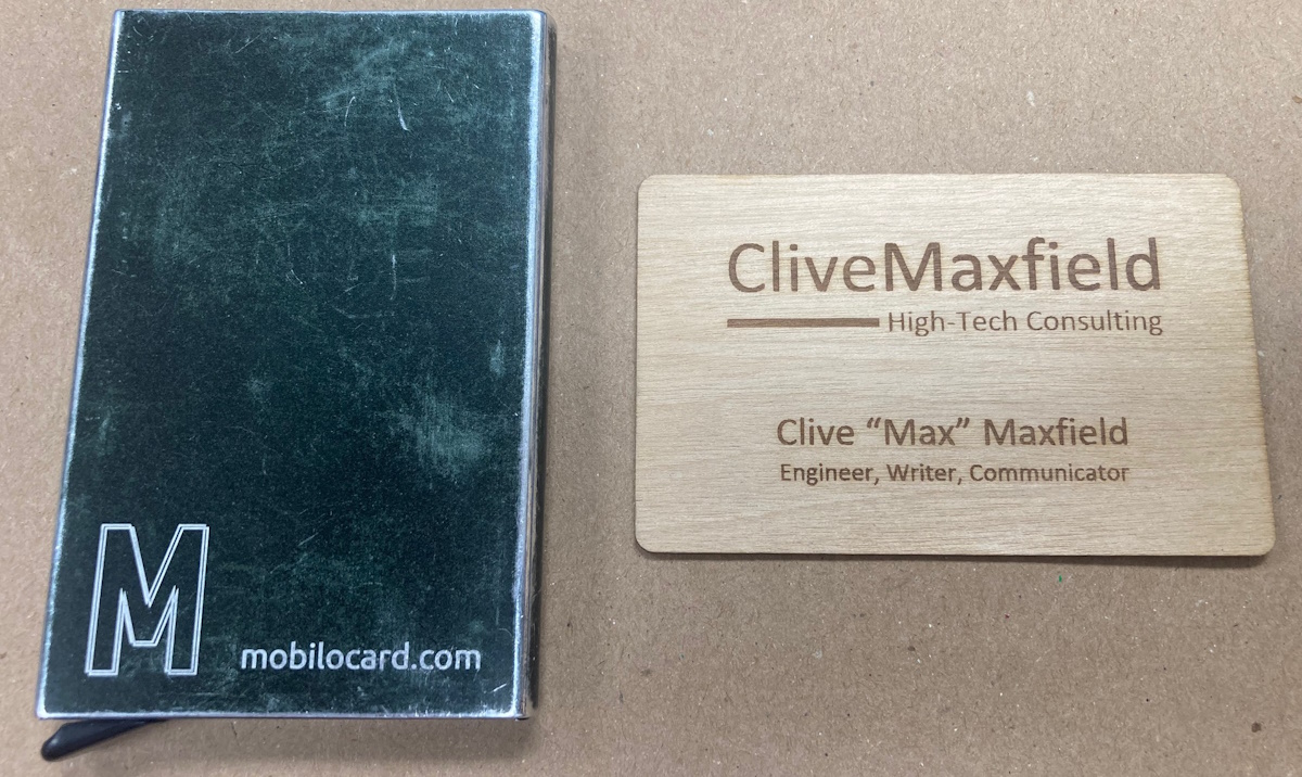
Meet my Mobilo card (right) and metal carrying case (left) (Source: Max Maxfield)
I opted for the Cool Beans-looking wooden version. Although this is only about 1mm thick, it contains an embedded NFC (Near Field Communication) chip. I also have a handy-dandy metal case to protect the card in my pocket. From the battered look of the case, you can see that we’ve been through some adventures together. Pulling the lever at the bottom of the case causes the card to leap out into my hand.
All I need to do is bring the card close to someone’s smartphone. This triggers the phone to launch a landing page pre-populated with my information (name, position, photo, website, LinkedIn, etc.). There’s also a QR code on the back that can be used by those who have NFC disabled.
The reason I mention this is that I was just chatting with Juergen Jaeger, who is Market Management Program Director for Siemens EDA Hardware-Assisted Verification Group. Try saying that ten times quickly. Now, there’s a man who could benefit from having a Mobilo Digital Business Card if ever there was one (you see, I told you my Mobilo mutterings were relevant).
The reason we were chatting was for Juergen to bring me up to speed on the latest and greatest intelligence regarding the Veloce proFPGA prototyping and verification platform (the full name is Veloce proFPGA CS, where the “CS” portion of the moniker stands for “Capacity System”).
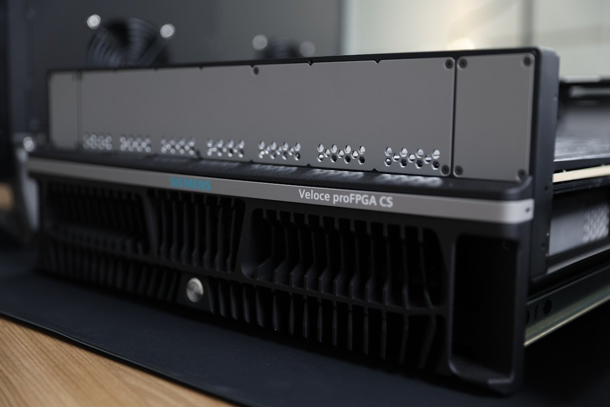
Siemens’ Veloce proFPGA CS is an advanced at-speed prototyping platform that takes full advantage of the benefits of FPGAs and multi-FPGA partitioning (Source: Siemens)
Before we go there, however, let’s briefly set the scene. One of the keys to Veloce proFPGA’s awesomeness is its magnificently modular architecture. This starts with a suite of FPGA Modules. Each module contains an FPGA, along with configuration circuitry, support logic, local power regulation, clocking resources, memory devices, high-speed connectors, and a management interface (circuitry for monitoring temperature, voltage, and current, as well as for coordinating with the system software for debugging and control).
Next up is a suite of Platform Boards (motherboards): the Uno, Duo, and Quad boards carry 1, 2, or 4 FPGA modules, respectively. These motherboards also provide extension sites, allowing external interfaces, memory, and I/O boards to be plugged in. Users can decide which FPGA modules they wish to use with their motherboard (the modules are designed so they can plug into any of the motherboards). Also (and I really like this bit), rather than being forced to purchase fully-populated motherboards, users can opt to start with a Duo board along with just 1 FPGA module, or a Quad with only 1, 2, or 3 modules, and then add more modules later.
Once you’ve decided on the system you want (motherboard + FPGA modules + extension boards + power/cables, etc.), you’ll typically want to install it in a Housing (i.e., a case or enclosure). These housings are designed to accommodate Uno, Duo, Quad motherboards, power supplies, and extension boards, and to provide side access to connectors, among other features. The resulting systems can be desktop-mountable or rack-mountable; in fact, they can even be portable, allowing you to perform tasks such as verifying a system running in an automobile, for example.
But wait, there’s more. In addition to the classic motherboard architecture, the Veloce proFPGA family now boasts a blade architecture flaunting QUAD Blades (with up to 4 FPGA Modules) and HEXA Blades (with up to 6 FPGA Modules). Each blade integrates not just the FPGA sockets but also high-performance backplane connectors, clocking, power distribution, and system management. Blades can run stand-alone on the desk (desktop housing) or be slotted into a rack backplane for multi-blade scaling.
Last, but certainly not least, is the Veloce proFPGA Software, which accepts the RTL for the design and automatically performs tasks such as partitioning, memory modeling, pin-multiplexing, debug IP insertion, creating constraint files, and more.
Now that we’ve set the scene, the latest FPGA module in the family features AMD’s Versal Premium VP1902 adaptive SoC. This has been described as the world’s biggest, boldest, largest, and scariest FPGA-based SoC. It’s designed specifically for the emulation and prototyping of complex next-generation chip designs, particularly those intended to handle AI and machine learning workloads. The VP1902 integrates a vast amount of logic capacity, high-speed memory bandwidth, and hardened IP for interfaces like PCIe Gen5 and Ethernet. It also employs a chiplet-based architecture to simplify routing and reduce latency.
The great thing about Veloce proFPGA is its scalability. You can start off with a desktop configuration consisting of an Uno motherboard with a single FPGA module, and you can end up with a rack containing ten fully populated HEXA Blades, which equates to 60 FPGA modules. To put this in perspective, 60 VP1902 modules equate to approximately 3 billion gates of capacity. And, of course, you can connect multiple of these racks together. Consider my mind boggled.
When we refer to “instrumentation” in the context of FPGA prototypes, we mean any additional debug and visibility logic inserted into the design (or provided by the prototyping platform) that enables us to observe, trace, and analyze internal signals, states, and events during execution.
The traditional approach is to provide a list of signals upfront. The system then modifies the design RTL to incorporate signal probes and monitors, trigger and trace logic, and performance counters and checkers, along with any other necessary visibility infrastructure.
The problem is, of course, that you’ve no sooner started your verification run when you discover you need to look at something that wasn’t on the list. “Oh dear,” you might say to yourself (or words to that effect). So, you can only imagine my delight to discover that the folks at Siemens have introduced a new “Probeless Debug” capability, which allows us to observe signals that we neglected to specify before we started.
Additionally, it would be remiss of us to neglect to note that Veloce proFPGA is but one member of the Veloce Platform triad, trio, or troika (as you prefer), the others being Veloce Strato+ and Veloce Primo (I introduced this ensemble a while back in my A Brave New World of Emulation and Software Prototyping column).
All I can say is “Phew!” (and I mean that most sincerely). We’ll end, as usual, with my asking you, “So, what do you think about all of this?”

