

Things continue to gain traction in “chiplet space” (where no one can hear you scream). In fact, before I forget, Chiplet Summit 2026 takes place in just a couple of weeks as I pen these words. The organizers say this is the place to “see and be seen” if you are in any way dabbling your toes in the chiplet waters (I’m paraphrasing, of course).
Not surprisingly, one of the keynote presentations at the Chiplet Summit will be given by Cadence, which is doing some very interesting things on the chiplet front. This presentation will be given by David Glasco, VP Compute Solutions Group at Cadence. David oversees hardware/software design and implementation of soft IP for AI, and his presentation will cover modular multi-die designs for AI, edge, and physical AI applications.
Hmmm, “physical AI applications.” Reading this made me think, “What’s that when it’s at home?” as people say in England. Fortunately, I was just chatting with Michael Posner, Sr Product Marketing Group Director, Chiplets & IP solutions at Cadence. Michael explained that physical AI is any system that performs AI processing at the edge, including autonomous vehicles, drones, and robots.
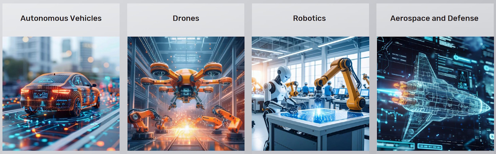
Physical AI systems are the next evolution in the AI journey (Source: Cadence)
Michael also noted that if you look at what the folks in Aerospace and Defense are doing with their edge AI, it’s fundamentally targeted at their autonomous vehicles, autonomous drones, and autonomous robotic systems, but they have some unique requirements for their physical AI, which is why Aerospace and Defense are typically assigned their own niche in the scheme of things.
As an aside, the phrase “physical AI systems” is relatively new and still emerging, rather than long-established or universally standardized. In fact, it wasn’t widely used in mainstream engineering or AI literature prior to the early-to-mid 2020s. Usage has grown quickly in the last few years, especially in discussions about robotics and autonomous machines, embodied AI and edge AI, and AI that senses, decides, and acts in the real world, not just in software.
Since Michael and I have both been around for a long time, we discussed how the current excitement over the term “multi-die” can be confusing for older engineers, since they’ve “been there, done that, and seen it all before.” On the off chance you’re interested:
- Multiple silicon dies mounted on a single ceramic substrate interconnected with thin-film metallization and wire bonds began to appear in the mid-1960s.
- Hybrid microelectronics matured (thick-film and thin-film on ceramic) in the 1970s, leading military, aerospace, and high-reliability computing to widely adopt multi-die ceramic hybrids.
- The formal term multi-chip module (MCM) gained traction in the 1980s, with high- end computers and defense electronics adopting MCM-C (ceramic) and MCM-D (thin-film-deposited dielectric) technologies.
- From the 1990s onwards, commercial high-performance processors and memory subsystems increasingly used ceramic MCMs, and this lineage leads directly to today’s chiplet and advanced packaging technologies.
The bottom line is that MCMs have been around for many years and are now powering infrastructure, data centers, AI, and high-performance computing (HPC). So, what’s the difference between a multi-die device like an MCM and a chiplet-based design, which is also somewhat confusingly known as a multi-die system?
In a crunchy nutshell, until recently, modern multi-die devices have almost invariably been created by behemoth companies that control every aspect of the design and packaging process, including the development of their own proprietary die-to-die communication interfaces (electrical and protocol).
By comparison, the vision for future chiplet-based multi-die systems is to be able to “mix and match” chiplets purchased on the open marketplace. Chiplets offer a system architecture strategy that supports yield optimization, process-node mixing, IP reuse across products, and scalable performance tiers. The die-to-die links in today’s chiplet-based designs are approaching on-chip interconnect density by means of technologies like silicon interposers (2.5D), hybrid bonding/3D stacking, and standardized die-to-die PHYs. In short, today’s chiplets blur the line between “multi-die” and “one big chip.”
Sad to relate, however, “we aren’t there yet.”
Where we actually are is at an intermediate stage—partway between the MCM past and the open chiplet marketplace future—waiting for standards for things like die-to-die interconnects and protocols to stabilize and mature. In the meantime, groups of companies are forming their own multi-die system ecosystems to get multi-die systems up-and-running now (see also my column, No Need to Delay—You Can Create Chiplet- Based Designs Today!).
Into this intriguing in-between world steps Cadence, proudly flaunting a tangible platform, a growing ecosystem, and—perhaps most significantly—the practical means to turn chiplet ambition into working silicon.
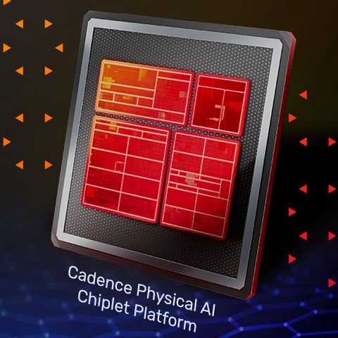
Cadence’s latest push into chiplets centers on what it calls a Physical AI Chiplet Platform. This is a configurable, multi-die architecture designed to bring real-time AI processing to edge-class physical AI systems. Rather than treating chiplets as isolated silicon components, Cadence is positioning the platform as a spec-driven, framework-based system that integrates CPU compute, AI acceleration, system connectivity, security, and debug into a cohesive multi-die environment. The intent is to shift chiplet development from a ground-up silicon exercise toward a more repeatable, packaging-centric integration flow, thereby shortening development cycles and enabling scalable product families built from common chiplet building blocks.
As depicted in the diagram below, at the architectural level, the platform combines an Arm-based compute subsystem (the CPU Chiplet), Cadence AI acceleration (the AI Chiplet), a configurable System Chiplet, and optional Domain-Specific Chiplets (typically created by the customer or by Cadence’s Custom Silicon Services, as discussed below), all interconnected through standards-aligned die-to-die technologies such as UCIe, cache-coherent and I/O-coherent network-on-chip (NoC) fabrics, and a unified chiplet framework that manages boot, security, debug, and lifecycle control across dies.
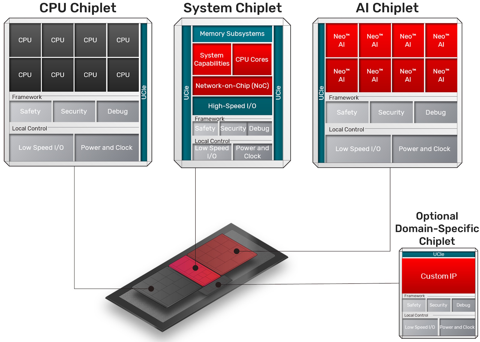
Cadence Physical AI Chiplet Platform (Source: Cadence)
This framework-centric approach is intended to move the industry beyond proprietary multi-die implementations toward interoperable, standards-driven chiplet ecosystems while still allowing customers to customize domain-specific chiplets or scale compute and AI resources as needed.
Recent announcements at CES 2026 extend this technical foundation into a broader Chiplet Spec-to-Packaged-Parts ecosystem, where Cadence collaborates with partners spanning compute IP, interconnect, memory, security, analytics, and foundry manufacturing to deliver pre-validated chiplet solutions and accelerate customer time to market.
Initial IP partners joining Cadence include Arm, Arteris, eMemory, M31 Technology, Silicon Creations, and Trilinear Technologies, as well as silicon analytics partner proteanTecs. To help reduce risk and streamline customer adoption, Cadence is collaborating with Samsung Foundry to build out a silicon prototype demonstration of the Cadence Physical AI Chiplet Platform, including pre-integrated partner IP on the Samsung Foundry SF5A process.
By combining Cadence IP and design expertise with partner technologies—alongside simulation, emulation, and physical-design tool flows—the company aims to reduce engineering risk, simplify integration, and provide a practical on-ramp to production-grade chiplet systems targeting physical AI, data-center, and HPC workloads.
Importantly, Cadence’s strategy also reflects a broader shift in its business model. Through expanded silicon realization and custom-design capabilities, the company can now act as an end-to-end implementation partner, helping customers configure, tape out, and package chiplet-based silicon—even while continuing to supply the underlying IP, tools, and integration framework.
For example, Cadence’s acquisition of Invecas strengthens its system realization and silicon services capabilities, which directly support the delivery of customer-specific chiplets and full multi-die systems. Speaking of which, Cadence’s Custom Silicon Services provides the operational mechanism to implement the Physical AI Chiplet Platform in real silicon, aligning perfectly with the company’s “spec-to-packaged-parts” ecosystem message. This services dimension positions Cadence not merely as an EDA vendor but as a system-realization enabler for the emerging chiplet economy.
Whether chiplets ultimately fulfill their long-promised vision of open, mix-and-match silicon remains to be seen, but the direction of travel now feels unmistakable. What was once the exclusive playground of semiconductor giants is steadily evolving into a broader ecosystem of reusable building blocks, shared standards, and collaborative innovation. I don’t know about you, but I find the ongoing developments in this area tremendously exciting.

